
Wideband-instrumentation-amplifier
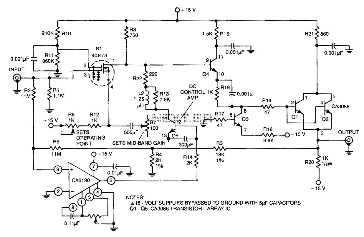
The circuit features an input resistance of 1 MΩ, a bandwidth extending from DC to approximately 35 MHz, and a gain of 10 times. Low-frequency gain is achieved using a CA3130 BiMOS operational amplifier configured as a single-supply amplifier. High-frequency gain is provided by a 40673 dual-gate MOSFET. The entire amplifier can be nulled by shorting the input to ground and adjusting resistor R9 to achieve zero DC output voltage.
The described circuit serves as a versatile amplifier capable of handling a wide range of frequencies. The CA3130 BiMOS op-amp is well-suited for low-frequency applications due to its high input impedance and low noise characteristics. Operating as a single-supply amplifier allows for simplified power supply requirements, making the design more compact and easier to integrate into various systems.
For high-frequency applications, the 40673 dual-gate MOSFET plays a crucial role in providing additional gain. This MOSFET configuration is particularly effective in RF applications, where maintaining signal integrity at higher frequencies is essential. The dual-gate configuration allows for improved control over the gain and enhances the amplifier's overall performance.
The adjustment process for nulling the amplifier is straightforward. By shorting the input to ground, any offset voltage at the output can be compensated by adjusting R9. This ensures that the amplifier operates at the desired output level, minimizing any DC offset that could affect performance.
Overall, this amplifier circuit is designed for applications requiring a combination of low and high-frequency amplification while maintaining a stable output. The careful selection of components and the ability to null the output voltage enhance the reliability and effectiveness of the circuit in various electronic systems.Has an input resistance of 1-MO, a bandwidth from de to about 35 MHz, and a gain of 10 times. Lowfrequency gain is provided by a CA3130 BiMOS op amp operated as a single-supply amplifier. High-frequency gain is provided by a 40673 dual-gate MOSFET. The entire amplifier is nulled by shorting the input to ground and adjusting R9 for zero de output voltage. 🔗 External reference