Zener Diodes
1. Definition and Basic Operation
Zener Diodes: Definition and Basic Operation
Fundamental Principles
A Zener diode is a heavily doped p-n junction semiconductor device designed to operate in the reverse breakdown region with a controlled and predictable voltage. Unlike conventional diodes that break down destructively, Zener diodes exploit quantum mechanical tunneling (Zener effect) and avalanche multiplication to maintain a stable voltage drop across their terminals.
The key operational characteristics are defined by:
- Zener voltage (VZ): The reverse breakdown voltage (typically 2.4V to 200V)
- Knee current (IZK): Minimum current required to sustain breakdown
- Zener impedance (ZZ): Dynamic resistance in breakdown region
Breakdown Mechanisms
Two distinct physical processes dominate depending on the doping concentration:
For low-voltage Zeners (< 5V), the Zener effect dominates where strong electric fields cause electrons to tunnel directly through the bandgap. Higher-voltage devices (> 5V) rely on avalanche breakdown, where carriers gain sufficient energy to create additional electron-hole pairs through collisions.
Current-Voltage Characteristics
The complete I-V curve exhibits three operational regions:
The reverse breakdown voltage remains nearly constant despite large current variations, making Zener diodes ideal for voltage regulation. The temperature coefficient (TC) of VZ varies with breakdown voltage:
Practical Considerations
In circuit design, the series current-limiting resistor (RS) must satisfy:
where IZ must remain between IZK (minimum knee current) and IZM (maximum rated current). Power dissipation is critical:
Modern Zener diodes often incorporate temperature compensation techniques using multiple junctions to achieve TC values below 0.05%/°C for precision references.
1.2 Key Characteristics and Parameters
Breakdown Voltage (VZ)
The defining characteristic of a Zener diode is its breakdown voltage (VZ), the reverse-bias voltage at which the diode begins conducting significantly. Unlike conventional diodes, which break down destructively, Zener diodes are designed to operate stably in this region. The breakdown mechanism is primarily due to the Zener effect for voltages below 5 V and avalanche breakdown for higher voltages. The voltage-current relationship in the breakdown region is modeled by:
where \( I_0 \) is the reverse saturation current, \( n \) is the ideality factor, and \( V_T \) is the thermal voltage (~26 mV at room temperature). In practice, manufacturers specify \( V_Z \) at a test current \( I_{ZT} \), typically a few milliamperes.
Dynamic Resistance (ZZ)
The dynamic resistance (ZZ) quantifies the diode's small-signal behavior in the breakdown region, defined as the slope of the V-I curve:
Lower \( Z_Z \) values indicate sharper breakdown characteristics, improving voltage regulation. For precision applications, \( Z_Z \) can be as low as 0.5 Ω, while general-purpose diodes may exhibit values up to 20 Ω. This parameter is frequency-dependent due to junction capacitance effects.
Power Dissipation and Thermal Considerations
The maximum power dissipation \( P_{max} \) is governed by:
where \( I_{Z(max)} \) is the maximum allowable current. Exceeding \( P_{max} \) leads to thermal runaway. The derating curve, typically linear above 25°C, follows:
with \( \kappa \) as the derating factor (mW/°C) and \( T_{ref} \) the reference temperature (usually 25°C). Proper heat sinking is critical for high-power Zeners (>1 W).
Temperature Coefficient (TC)
The temperature coefficient (TC) describes \( V_Z \)'s drift with temperature, expressed in %/°C or mV/°C. The TC varies nonlinearly with \( V_Z \):
- Below 5 V: Negative TC (Zener effect dominates)
- ~5 V: Near-zero TC (Zener and avalanche effects cancel)
- Above 5 V: Positive TC (avalanche effect dominates)
Precision voltage references often use series-connected Zeners with complementary TCs for compensation.
Junction Capacitance (CJ)
The depletion-layer capacitance \( C_J \) impacts high-frequency performance:
where \( C_{J0} \) is zero-bias capacitance, \( V_R \) is reverse voltage, \( \phi_0 \) is the built-in potential (~0.7 V for Si), and \( m \) depends on doping profile (0.5 for abrupt junctions). Low-capacitance Zeners (<1 pF) are essential for RF applications.
Noise Characteristics
Zener diodes exhibit broadband noise in breakdown, with spectral density increasing with current. The noise voltage \( v_n \) follows:
where \( K \), \( a \), and \( b \) are empirical constants. Low-noise references often employ buried-Zener structures or active filtering.
Long-Term Stability and Aging
Metallurgical changes cause \( V_Z \) drift over time, approximated by:
with \( A \) and \( B \) material-dependent. High-stability references use accelerated aging (burn-in) at elevated temperatures to stabilize the crystal lattice before deployment in precision circuits.
Breakdown Mechanisms: Zener vs. Avalanche
Zener diodes exhibit two distinct breakdown mechanisms—Zener breakdown and avalanche breakdown—each dominating under different conditions of reverse bias and doping concentration. The transition between these mechanisms is governed by quantum tunneling and impact ionization, respectively.
Zener Breakdown
Zener breakdown occurs in heavily doped p-n junctions (typically with doping concentrations exceeding 1018 cm−3) at relatively low reverse voltages (VZ < 5 V). The high electric field (E > 106 V/cm) across the narrow depletion region enables electrons to tunnel directly from the valence band of the p-region to the conduction band of the n-region. The tunneling probability Ptunnel is derived from the Wentzel-Kramers-Brillouin (WKB) approximation:
where m* is the effective electron mass, Eg is the bandgap, and E is the electric field. This mechanism exhibits a negative temperature coefficient (∂VZ/∂T < 0) due to bandgap narrowing at higher temperatures.
Avalanche Breakdown
Avalanche breakdown dominates in moderately doped diodes (1016–1017 cm−3) at higher voltages (VZ > 7 V). Here, carriers gain sufficient kinetic energy to ionize lattice atoms via impact ionization, creating electron-hole pairs that multiplicatively amplify the reverse current. The avalanche multiplication factor M is given by:
where VBR is the breakdown voltage and n ranges from 3 to 6 for silicon. Unlike Zener breakdown, avalanche exhibits a positive temperature coefficient (∂VZ/∂T > 0) due to reduced carrier mean free paths at elevated temperatures.
Crossover Region (5–7 V)
In diodes with breakdown voltages between 5–7 V, both mechanisms coexist, resulting in a near-zero temperature coefficient. This property is exploited in precision voltage references like the LM399, where temperature stability is critical. The total current density J in this regime combines tunneling and avalanche components:
Practical Implications
- Low-voltage Zener diodes (<5 V) are preferred for noise-sensitive applications due to their quieter breakdown characteristic.
- Avalanche diodes (>7 V) handle higher power dissipation but require thermal management to prevent runaway.
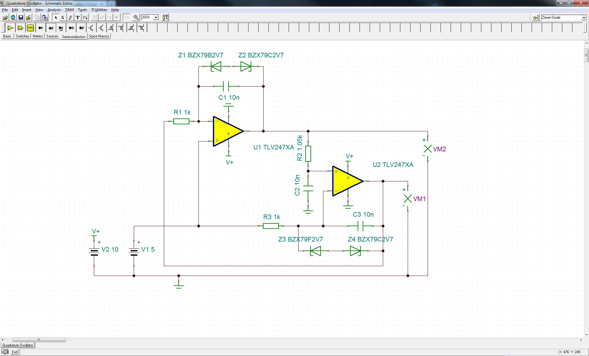
- 6.2 V diodes (e.g., 1N821) leverage the crossover region for minimal drift in voltage references.
2. Voltage Regulation Circuits
Voltage Regulation Circuits
Operating Principle of Zener Diodes in Regulation
A Zener diode operates in reverse breakdown to maintain a stable voltage across its terminals. When reverse-biased beyond the Zener voltage (VZ), the diode enters the avalanche or Zener breakdown region, where a small change in current results in minimal voltage variation. This characteristic makes it ideal for voltage regulation.
Here, rZ is the dynamic impedance of the Zener diode, typically in the range of a few ohms to tens of ohms. Lower rZ values yield better regulation performance.
Basic Zener Voltage Regulator
The simplest voltage regulator consists of a Zener diode in parallel with the load and a series resistor (RS) to limit current. The resistor must be chosen such that the Zener remains in breakdown over the expected input voltage (Vin) and load current (IL) range.
For optimal performance, IZ should be maintained within the manufacturer-specified range (IZ(min) to IZ(max)). Exceeding IZ(max) risks thermal runaway, while falling below IZ(min) results in poor regulation.
Line and Load Regulation
Line regulation quantifies the circuit's ability to maintain Vout despite variations in Vin:
Load regulation measures stability against changes in load current:
In both cases, minimizing rZ and selecting an appropriate RS are critical for high-performance regulation.
Practical Considerations and Enhancements
For improved regulation, a transistor can be added to form a Zener-follower regulator. The transistor offloads current-handling from the Zener, reducing power dissipation and improving load regulation:
where VBE is the base-emitter voltage drop of the transistor. Further refinements include using operational amplifiers for active feedback control, achieving sub-1% regulation accuracy.
Thermal Effects and Stability
Zener voltage exhibits a temperature coefficient (TC), typically ranging from ±0.05%/°C to ±0.1%/°C. For precision applications, temperature-compensated Zener diodes or buried-Zener references (e.g., LM399) are employed, offering TC values below 5 ppm/°C.
2.2 Overvoltage Protection
Zener diodes are widely employed in overvoltage protection circuits due to their precise reverse breakdown characteristics. When the voltage across the Zener diode exceeds its breakdown voltage (VZ), it enters the avalanche or Zener breakdown region, effectively clamping the voltage to VZ. This property is exploited to safeguard sensitive electronic components from voltage transients.
Working Principle
In an overvoltage protection circuit, the Zener diode is connected in parallel with the load. Under normal operating conditions, the input voltage (Vin) remains below VZ, and the diode operates in reverse bias with minimal leakage current. However, if Vin exceeds VZ, the diode conducts heavily, diverting excess current away from the load and limiting the voltage across it.
Design Considerations
The series resistor (RS) is critical in determining the current through the Zener diode. It must be chosen such that:
- The Zener operates within its specified power dissipation limits.
- Sufficient current is available to maintain regulation under worst-case conditions.
where IZ(max) is the maximum allowable Zener current, derived from the power rating:
Transient Response and Clamping Speed
Zener diodes exhibit fast response times (typically nanoseconds), making them effective against high-frequency transients. The junction capacitance (CJ) and series inductance influence the clamping speed, with lower values preferred for high-speed applications.
Practical Applications
Common implementations include:
- Voltage clamping in power supply rails.
- ESD protection for integrated circuits.
- Surge suppression in communication lines.
Limitations
While effective, Zener-based protection has drawbacks:
- Limited energy absorption capability compared to TVS diodes.
- Degradation under repetitive high-energy transients.
- Temperature dependence of VZ.
Waveform Clipping and Clamping
Zener Diode as a Waveform Clipper
Zener diodes are widely used in waveform clipping circuits to limit signal amplitudes. When the input voltage exceeds the Zener breakdown voltage VZ, the diode conducts, clamping the output to VZ. For a sinusoidal input Vin = Vpsin(ωt), the output waveform Vout is clipped symmetrically or asymmetrically depending on the circuit configuration.
In a dual-Zener clipping circuit, two diodes are arranged antiparallel to clip both positive and negative peaks. The clipped waveform retains the input frequency but exhibits flat tops and bottoms at ±VZ.
Biased Clipping Circuits
Adding a DC bias voltage Vbias in series with the Zener diode shifts the clipping threshold:
This allows precise control over clipping levels, useful in signal conditioning and overvoltage protection. The bias can be implemented using voltage dividers or precision references.
Waveform Clamping with Zener Diodes
Zener-based clamping circuits shift the DC level of AC signals without altering waveform shape. A typical configuration combines a capacitor for AC coupling and a Zener diode to establish the DC reference:
The capacitor charges to the peak input voltage minus VZ, effectively adding a DC offset. This technique is essential in video signal processing and analog computing where DC restoration is required.
Practical Considerations
- Dynamic resistance: The finite slope of the Zener's I-V curve causes minor waveform distortion near the clipping threshold.
- Temperature coefficients: Breakdown voltage variations with temperature affect clipping precision in critical applications.
- Power dissipation: Must satisfy PZ = IZVZ ≤ rated power, requiring current-limiting resistors.
For high-frequency signals, the junction capacitance of the Zener diode becomes significant, potentially causing phase shift and attenuation before clipping occurs.
Advanced Applications
In precision instrumentation, Zener clipping circuits with operational amplifiers create soft clipping characteristics. The op-amp's feedback network linearizes the transition region while maintaining sharp clipping thresholds. Such circuits achieve total harmonic distortion (THD) below 0.1% in audio processing applications.
For transient suppression, fast-acting Zener diodes with nanosecond response times clip voltage spikes in communication lines. The energy absorption capability is given by:
where t1 to t2 is the transient duration. Modern Zener arrays handle multi-kilowatt pulses for industrial surge protection.
3. Selecting the Right Zener Diode
3.1 Selecting the Right Zener Diode
Key Parameters for Selection
When selecting a Zener diode, the primary parameters to consider are the Zener voltage (VZ), power dissipation (PZ), tolerance, and temperature coefficient (TC). The Zener voltage is the reverse breakdown voltage at which the diode begins to conduct, and it must match the desired regulation voltage. Power dissipation, given by:
determines the maximum current the diode can handle before thermal failure. For example, a 5.1V Zener diode rated at 1W can safely conduct up to approximately 196 mA. Tolerance specifies the allowable deviation from the nominal VZ, typically ranging from ±1% to ±10%. The temperature coefficient indicates how VZ varies with temperature, critical for precision applications.
Dynamic Resistance and Load Regulation
The dynamic resistance (rZ) of a Zener diode affects its ability to maintain a stable output voltage under varying load conditions. It is defined as the slope of the V-I curve in the breakdown region:
Lower rZ values (e.g., 1–10 Ω) are preferable for tight voltage regulation. For instance, a diode with rZ = 5 Ω and IZ = 10 mA will exhibit a voltage change of only 50 mV for a ±10 mA current variation. This parameter is particularly important in power supply designs where load current fluctuations are expected.
Thermal Considerations and Derating
Zener diodes dissipate power as heat, and their maximum ratings must be derated at elevated temperatures. The junction-to-ambient thermal resistance (θJA) dictates the temperature rise per watt of dissipated power:
where TJ is the junction temperature and TA is the ambient temperature. Exceeding the maximum junction temperature (typically 150–200°C) can lead to catastrophic failure. For example, a diode with θJA = 100°C/W operating at 0.5W in a 25°C environment will reach a junction temperature of 75°C. Proper heat sinking or current limiting may be necessary in high-power applications.
Zener Voltage vs. Current Characteristics
The relationship between Zener voltage and current is nonlinear, following an exponential trend in the breakdown region. For a first-order approximation, the voltage-current relationship can be modeled as:
where VZ0 is the extrapolated voltage at zero current. This linearized model is valid only for small current variations around the test current (IZT) specified in the datasheet. For wide current ranges, higher-order models or empirical data must be used.
Practical Selection Criteria
- Voltage Accuracy: Choose tighter tolerances (±1–2%) for precision references.
- Power Handling: Ensure PZ exceeds worst-case dissipation, including transients.
- Temperature Stability: Low TC (<±0.05%/°C) is critical for temperature-sensitive applications.
- Package Limitations: Surface-mount diodes may have lower power ratings than through-hole counterparts.
For example, in a 12V automotive voltage regulator, a 15V Zener with a 5W rating and a ±5% tolerance might be selected to account for load dump transients while maintaining adequate regulation.
3.2 Thermal Management and Power Dissipation
Zener diodes, when operated in reverse breakdown, dissipate power as heat due to the product of the Zener voltage (VZ) and the current (IZ). The total power dissipation (PD) is given by:
Exceeding the maximum rated power dissipation (PD(max)) leads to thermal runaway and permanent damage. Manufacturers specify PD(max) at a reference temperature (typically 25°C), derated linearly with increasing junction temperature (TJ). The derating curve follows:
where Tmax is the maximum allowable junction temperature (often 150°C–200°C for silicon devices).
Thermal Resistance and Heat Sinking
The junction-to-ambient thermal resistance (θJA) determines the temperature rise per watt dissipated. For a Zener diode mounted on a PCB:
where TA is the ambient temperature. To minimize TJ, reduce θJA by:
- Using a heatsink (lowering θJC + θCS + θSA)
- Increasing copper pour area on PCBs
- Forced air cooling for high-power applications
Transient Thermal Response
Under pulsed operation, the thermal time constant (Ï„th) of the diode package delays junction temperature rise. The transient thermal impedance (Zth(t)) models this behavior:
For short pulses (t ≪ τth), the effective power handling increases. Datasheets often provide Zth curves for duty cycle adjustments.
Practical Design Considerations
In voltage regulator circuits, ensure:
- Current limiting: A series resistor (RS) restricts IZ to safe levels:
$$ R_S = \frac{V_{in} - V_Z}{I_Z} $$
- Temperature compensation: For precision references, use compensated Zeners or external circuitry to counteract VZ drift (~2 mV/°C).
- Parallel devices: Distribute power dissipation across multiple Zeners for high-current applications.
3.3 Common Pitfalls and Troubleshooting
Thermal Runaway and Power Dissipation
Zener diodes are susceptible to thermal runaway when operating near their maximum power dissipation limit. The power dissipated in a Zener diode is given by:
where IZ is the Zener current and VZ is the Zener voltage. As temperature increases, the Zener breakdown voltage decreases, leading to higher current draw. This positive feedback loop can cause catastrophic failure if not properly managed. Engineers should:
- Derate power specifications by at least 20% for reliable operation
- Use adequate heatsinking for power Zeners (>1W)
- Monitor junction temperature in critical applications
Incorrect Biasing and Load Regulation
A common design error involves insufficient current through the Zener to maintain regulation. The minimum Zener current IZK (knee current) must be maintained under all load conditions. For a series resistor RS with input voltage VIN:
where IL is the load current. Failure to account for IL variations leads to either:
- Loss of regulation (too high RS)
- Excessive power dissipation (too low RS)
Noise and Instability in Precision Circuits
Zener diodes exhibit significant noise in breakdown operation, particularly in the 5-10V range where both avalanche and Zener mechanisms contribute. The noise spectral density follows:
where K is the flicker noise coefficient (typically 10-12 to 10-10 V2/Hz), α ≈ 1, and S0 is the white noise floor. For low-noise applications:
- Use buried-Zener references (e.g., LM399) instead of conventional Zeners
- Implement proper bypassing with low-ESR capacitors
- Consider forward-biased diodes for references below 5V
Voltage Tolerance and Temperature Coefficients
Zener voltage specifications often mislead designers. The nominal VZ typically has ±5% tolerance at a specific test current, with significant variation across:
- Temperature (TC ≈ +2mV/°C for VZ < 5V, negative TC for VZ > 7V)
- Operating current (dynamic impedance effects)
- Aging (up to 0.1% drift per 1000 hours)
The temperature coefficient can be estimated by:
Transient Response and Protection
Zener diodes used for voltage clamping must handle fast transients without failure. The energy rating is critical:
where IPP is the peak pulse current and tPW is the pulse width. Common oversights include:
- Ignoring lead inductance effects in high-speed clamping
- Underestimating repetitive pulse energy ratings
- Neglecting the diode's thermal time constant
4. Temperature Coefficient and Stability
4.1 Temperature Coefficient and Stability
The temperature coefficient (CT) of a Zener diode quantifies how its breakdown voltage (VZ) varies with temperature. This parameter is critical in precision voltage reference applications, where thermal stability directly impacts circuit performance. The coefficient is typically expressed in millivolts per degree Celsius (mV/°C) or as a percentage change per degree (%/°C).
Breakdown Mechanism Dependence
Zener diodes exhibit distinct temperature behaviors based on their dominant breakdown mechanism:
- Avalanche breakdown (VZ > 5.6V): Positive temperature coefficient (0.05% to 0.1%/°C) due to increased lattice scattering at higher temperatures.
- Zener breakdown (VZ < 5V): Negative temperature coefficient (-0.02% to -0.05%/°C) caused by reduced bandgap energy with temperature.
- 5V-6V transition region: Near-zero coefficient as the two effects cancel each other.
Mathematical Modeling
The temperature-dependent Zener voltage can be expressed as:
Where VZ0 is the nominal breakdown voltage at reference temperature T0 (usually 25°C). For precision analysis, the second-order coefficient must be considered:
where α is the first-order coefficient and β represents curvature.
Stability Optimization Techniques
Several methods exist to improve thermal stability in Zener-based circuits:
- Series compensation: Combining forward-biased diodes (negative CT) with avalanche Zeners to achieve net-zero coefficient.
- Temperature-controlled environments: Ovenization or thermal feedback loops maintain constant junction temperature.
- Current regulation: Maintaining constant power dissipation through precise bias current control.
Compensation Circuit Analysis
The optimal number of compensating diodes (N) for a given Zener can be derived from:
where Vd is the diode forward voltage (≈0.7V for Si) and CT,diode ≈ -2mV/°C.
Practical Considerations
In voltage reference designs, the long-term stability of Zener diodes depends on:
- Junction temperature uniformity (affected by package thermal resistance)
- Burning-in effects (voltage drift during initial operation)
- Load current variations (impacting self-heating)
High-precision references often use buried Zener structures (e.g., LM399) that achieve temperature coefficients below 0.0005%/°C through substrate isolation and optimized doping profiles.
4.2 Dynamic Impedance and Frequency Response
Dynamic Impedance in Zener Diodes
The dynamic impedance (ZZ) of a Zener diode quantifies its small-signal resistance when operating in the breakdown region. Unlike the static resistance, which is derived from DC characteristics, dynamic impedance is frequency-dependent and governs the diode's response to AC perturbations. It is defined as:
where VZ is the Zener voltage and IZ is the current through the diode. For practical Zener diodes, ZZ typically ranges from 1Ω to 100Ω, decreasing with higher bias currents due to enhanced carrier mobility in the breakdown region.
Frequency Dependence and Equivalent Circuit
At high frequencies, parasitic elements dominate the diode's behavior. The small-signal equivalent circuit includes:
- Dynamic resistance (rz) – The real component of ZZ, inversely proportional to the slope of the I-V curve in breakdown.
- Junction capacitance (Cj) – Arises from the depletion region, modeled in parallel with rz.
- Series inductance (Ls) – Stray inductance from leads and bonding wires.
where ω = 2πf. The impedance exhibits a minimum at the self-resonant frequency (fSR), where inductive and capacitive reactances cancel:
Practical Implications
In voltage regulation circuits, excessive dynamic impedance causes output ripple and poor transient response. For instance, a 5.6V Zener with ZZ = 5Ω under 10mA bias will exhibit a 50mV variation for a 10mA load transient. High-frequency applications (e.g., RF clamping) require Zeners with low Cj (< 10pF) to avoid signal attenuation.
Measurement Techniques
Dynamic impedance is measured using:
- Network analyzers – Sweep frequency while monitoring impedance phase and magnitude.
- Pulsed I-V testing – Apply fast current steps and measure voltage settling time.
The plot above illustrates the typical impedance-frequency relationship, showing the resonant dip at fSR.
4.3 Zener Diodes in Precision Circuits
Voltage Reference Stability
Zener diodes are widely employed as precision voltage references due to their predictable breakdown characteristics. The temperature coefficient (TC) of a Zener diode is critical in precision applications. For Zeners operating in the 5–6 V range, the temperature coefficient approaches zero due to the cancellation of avalanche and Zener effects. Outside this range, TC becomes non-negligible:
where α is a material-dependent constant (~2 mV/°C for silicon) and VZ0 is the zero-TC breakdown voltage (~5.6 V). For improved stability, compensated Zener references (e.g., LM399) combine a Zener with a forward-biased diode to cancel residual temperature dependencies.
Noise Considerations
Zener diodes exhibit two primary noise mechanisms in precision circuits:
- Avalanche noise: Broadband white noise proportional to the breakdown current
- Flicker noise: 1/f noise dominant at lower frequencies
The total noise spectral density can be modeled as:
where rz is the dynamic impedance, Cj is the junction capacitance, and Kf, a, b are empirical constants. In precision voltage references, this noise is typically reduced through:
- Current derating (operating below maximum IZ)
- Low-pass filtering
- Using buried-Zener structures (e.g., LTZ1000)
Dynamic Impedance Effects
The small-signal impedance of a Zener diode (rz = dV/dI) affects both line regulation and transient response. For a typical 6.2 V Zener:
where η is the ideality factor (~1–2), VT is the thermal voltage, and Rs is the series resistance. In precision applications, this impedance interacts with external components:
The output impedance seen by the load (Zout) becomes:
Long-Term Drift Mechanisms
Precision Zener references exhibit three primary drift mechanisms:
| Mechanism | Time Constant | Typical Magnitude |
|---|---|---|
| Thermal hysteresis | Hours-days | 5–50 ppm |
| Electromigration | Months-years | 10–100 ppm/year |
| Surface charge | Weeks-months | 2–20 ppm |
Buried-Zener references reduce these effects by isolating the active junction from surface states and contaminants.
Practical Implementation Example
A precision 10.000 V reference using a LTZ1000 demonstrates key design considerations:
* LTZ1000 Precision Reference
VIN 1 0 DC 15
R1 1 2 12K
Q1 2 3 4 2N3904
R2 3 0 70K
DZ1 4 0 LTZ1000
C1 4 0 10u
.model LTZ1000 D(Is=1e-12 BV=6.3 IBV=1m)
The circuit maintains ±0.05 ppm/°C stability through:
- Thermal regulation (Q1 as heater)
- Subsurface breakdown (buried Zener)
- Precision resistor ratios (R1/R2)
5. Recommended Books and Papers
5.1 Recommended Books and Papers
- Electronics Handbook/Components/Diodes/Zener - Wikibooks — Zener diodes are widely used to regulate the voltage across a circuit. When connected in parallel with a variable voltage source so that it is reverse biased, a Zener diode conducts when the voltage reaches the diode's reverse breakdown voltage. ... For example, the common BZX79C5V6 [1] device, a 5.6 V 0.5 W Zener diode, has a recommended ...
- PDF Electronics Principles and Devices Zener Diode — Zener Diode Instructor: Dr. Rand Basil Alhashimie. 2 Outline •Introduction of Zener Diode •Voltage-Current Characteristics for Zener Diode •Zener Diode Breakdown ... Calculate the zener impedance if the change in zener voltage is 100 mV for a 20 mA change in zener current
- COMPLETE GUIDE TO SEMICONDUCTOR DEVICES - Wiley Online Library — Zener Diode Step-Recovery Diode. Fasl Snap-Back Diode Anisotype Heterojunction Varactor. Varactor Diode. :-Recovery Diode. Varicap Diode Snap-Off Diode 11 11 11 12 18 20 20 20 22 2. p-i-n Diode 24 3. Schottky-Barrier Diode 31 Metal-Semiconductor Junction. Poin t Contact. Surface-Barrier Diode. Hot-Carrier Diode. Hot-Electron Diode 3.5.1 Mott ...
- PDF ECE-291 Electronic Engineering Lecture #2 Diode Applications ... - BU — Electronic Engineering l-a 1 . ... Power Supply Regulators Zener Diode LED Photodiode 2 5 l-a. DIODE APPLICATIONS 3 l-a 5. Rectifiers Half-wave Rectifiers l-a 5 4 . Half-wave Rectifier Operation l-a 5 5 . Average Voltage & PIV • The peak inverse voltage (PIV) equals the peak value of the input voltage ... • Zener Regulation with a Variable ...
- PDF Microelectronic Circuits - img.electronicdesign.com — 4.3.6 The Ideal-Diode Model 194 4.3.7 The Small-Signal Model 195 4.3.8 Use of the Diode Forward Drop in Voltage Regulation 200 4.4 Operation in the Reverse Breakdown Region—Zener Diodes 202 4.4.1 Specifying and Modeling the Zener Diode 203 4.4.2 Use of the Zener as a Shunt Regulator 204 4.4.3 Temperature Effects 206 4.4.4 A Final Remark 207
- PDF How to use a voltage reference as a voltage regulator - Texas Instruments — non-temperature-compensated diodes. Figure 2. Zener Diodes Typically Require a More than a Few Milliamps to Reach Vz Ohm's law and Joule's law dictate the power losses across the shunt resistor, which affects overall system losses and temperatures. As an example, with a 12V input, using a 2.5V Zener diode would require a 1.9kΩ
- Semiconductor Diode - SpringerLink — A 5V Zener diode with a minimum current requirement of 10 mA is to be used in a voltage regulator. The supply voltage is 18 V, and the variable load current has a maximum value of 25 mA. Calculate the minimum power rating of the Zener diode, the required series resistance and the minimum load resistance that can be connected to the regulator.
- PDF voltage regulators zeners — Zener Diode Voltage Regulators 1 by Kenneth A. Kuhn April 3, 2009, rev. April 7, 2013 Introduction A Zener diode is a PN junction that has been specially made to have a reverse voltage breakdown at a specific voltage. Its characteristics are otherwise very similar to common diodes.
- (PDF) Hand Book of Electronics - ResearchGate — 14.3.1 Zener Diode Shunt Regulator . ... In this paper, a new approach for the control of superposition ratio of odd harmonic wave into output voltage feedback control and improvement on voltage ...
- PDF Special-Purpose Diodes - talkingelectronics.com — In other words, the zener diode operated in this region will have a relatively constant voltage across it, regardless of the value of current through the device. This permits the zener diode to be used as a voltage regulator. For detailed discussion on zener diode, the reader may refer to chapter 6 of this book. 7.2 Light-Emitting Diode (LED)
5.2 Online Resources and Datasheets
- PDF NZ9F2V4ST5G, SZNZ9F2V4ST5G SERIES Zener Voltage Regulators - onsemi — This series of Zener diodes is packaged in a SOD−923 surface mount package. They are designed to provide voltage regulation ... NZ9F4V7ST5G E 4.55 4.75 5 100 800 0.5 2 1 −3.5 0.2 150 SZ, NZ9F5V1ST5G F 4.989 5.2 5 80 500 0.5 2 1.5 −2.7 1.2 130 ... "Typical" parameters which may be provided in onsemi data sheets and/or ...
- PDF BZX79C2V4 - Zener Diodes - onsemi — DATA SHEET www.onsemi.com ... BZX79C2V4/D Zener Diodes BZX79C2V4 - BZX79C18 ABSOLUTE MAXIMUM RATINGS (Note 1) Values are at TA = 25°C unless otherwise noted. Symbol Parameter Value Unit PD Power Dissipation @ TL ≤ 75°C, Lead Length = 3/8″ ... BZX79C2V7 2.5 2.9 5 100 75 1 −3.5 0 230 BZX79C3V3 3.1 3.5 5 95 25 1 −3.5 0 200
- PDF Small Signal Zener Diodes - media.digikey.com — Small Signal Zener Diodes Features • Silicon planar power zener diodes †These diodes are also available in other case styles and other configurations ... BZT52C2V7-V-G Y2 2.5 2.9 75 (< 83) < 500 5 - 9 to - 4 - 113 134 BZT52C3V0-V-G Y3 2.8 3.2 80 (< 95) < 500 5 - 9 to - 3 - 98 118
- BZT52-B5V1 (Single Zener diodes in a SOD123 package) - Nexperia — Cooling Fan Electronic Fuel Injection Fluid pump (12 V) Electrification (xEV powertrain) ... 5 : 2% : 5 : 5.2 : 250 : 590 : 40 : 150 : single : Package. Type number Orderable part number, (Ordering code (12NC)) ... Single Zener diodes: Data sheet: 2024-02-06: AN90063: Questions about package outline drawings: Application note:
- 5.2 V Zener Diodes Datasheets - Mouser - Mouser Electronics — 5.2 V Zener Diodes are available at Mouser Electronics. Mouser offers inventory, pricing, & datasheets for 5.2 V Zener Diodes. Skip to Main Content (800) 346-6873. Contact Mouser (USA) (800) 346-6873 | Feedback. Change Location. English. Español $$ USD United States. Please confirm your currency selection: Mouser Electronics - Electronic ...
- 5.2 V Zener Diodes - Mouser - Mouser Electronics — 5.2 V Zener Diodes are available at Mouser Electronics. Mouser offers inventory, pricing, & datasheets for 5.2 V Zener Diodes. Skip to Main Content (800) 346-6873. Contact Mouser (USA) (800) 346-6873 | Feedback. Change Location. English. Español $$ USD United States. Please confirm your currency selection: Mouser Electronics - Electronic ...
- PDF Zener Diodes BZG05C-SERIES — Zener Diodes BZG05C-SERIES ZDP0023A www.gmesemi.com 4 Product Specification Package Outline Dimensions (Unit: mm) Mounting Pad Layout (Unit: mm) Ordering Information Part Number Package Shipping Quantity BZG05C- SERIES SMA 5000 / Tape & Reel ... 5 / 2. 1 5 0. 2 0 T Y P. 0. 2 0 M A X. 4 .0 6 .5 1. 7 1. 6 7 2.08 4.18. Title: BZG05C-SERIES
- BZT52C5V6 datasheet - Zener Diode. Device Marking : W9 - DigChip — Features: *500mw Power Dissipation *Ideal for Surface Mountted Application *Zener Breakdown Voltage Range to 51V. Mechanical Data: *Case : SOD-123 Molded plastic *Terminals: Solderable per MIL-STD-202, Method 208 *Polarity: Cathode Indicated by Polarity Band *Marking: Marking Code (See Table on Page 3) *Weigh: 0.01grams(approx)
- 5.2 V Single Zener Diodes | Zener | Diodes | Electronic Components ... — Zener diodes are designed for operation in a reverse-breakdown mode and are characterized according to their behavior when used in this fashion. Useful as a voltage reference or for voltage limiting purposes, they are also capable of functioning as a one-way valve for current flow in the manner of rectifier diodes, though their behavior in this ...
- PDF Zener Diodes - Vishay Intertechnology — 1N4728A to 1N4761A www.vishay.com Vishay Semiconductors Rev. 2.7, 07-Nov-2024 3 Document Number: 85816 For technical questions within your region: [email protected], [email protected], [email protected]
5.3 Experimentation and Lab Guides
- Understanding Zener and LED Diodes: Voltage Regulation Lab Guide ... — 1 Centennial College ELECTRICAL ENGINEERING TECHNICIAN Course: EET-129 Electronics 1 Name (Please Print): EBIN SEBASTIAN Student Number: 300934644 Date: JULY 31 2024 LAB # 6 SPECIAL PURPOSE DIODES (ZENER AND LED) Small-signal and rectifier diodes are never intentionally operated in the breakdown region because this may damage them. A Zener diode is different; it is a silicon diode that the ...
- ECE102L Experiment 5.pdf - EXPERIMENT 5: ZENER DIODE AND... - Course Hero — EXPERIMENT 5: ZENER DIODE AND VOLTAGE REGULATION Lauguico, Christine S. B.S. Electronics Engineering Introduction When a reverse bias voltage of a PN junction is continually increasing, zener voltage occurs - voltage extends at which junction breakdown and current through the diode increases to a high value. In this case, zener diode or " breakdown diode " is designed to have a low and ...
- PDF ECE340 Lab Manual — %PDF-1.6 %âãÃÓ 7772 0 obj > endobj 7782 0 obj >/Filter/FlateDecode/ID[4C1BE245589EE144A3549DF558DC8BBC>84A570366A2CAD4293164910158EE28B>]/Index[7772 16]/Info 7771 ...
- Group 5 - Laboratory Report - Experiment 4 | PDF | Rectifier | Diode — GROUP-5_LABORATORY-REPORT_EXPERIMENT-4 - Free download as Word Doc (.doc / .docx), PDF File (.pdf), Text File (.txt) or read online for free. The document is a laboratory report that examines the properties and behavior of Zener diodes and DC power supplies. It includes data tables showing how the voltage and current across Zener diodes change with varying voltage sources.
- EE0015 Lab Activity 4 | PDF | Light Emitting Diode | P-N Junction — EE0015-Lab-Activity-4 - Free download as Word Doc (.doc / .docx), PDF File (.pdf), Text File (.txt) or read online for free. This document provides instructions for an activity to study the characteristics of light-emitting diodes (LEDs) and Zener diodes. The activity has students conduct experiments to determine: 1) The voltage and current required to turn on an LED and achieve "good brightness".
- PDF THEORY - Anna University — Laboratory ESC 0 0 4 4 2 8 BS3171 Physics and Chemistry Laboratory BSC 0 0 4 4 2 ... &Germanium - PN Junction Diodes, Zener Diode -Characteristics Applications - Bipolar Junction Transistor-Biasing, JFET, SCR, MOSFET,IGBT - Types, I-V Characteristics and Applications, ... Assembling and testing electronic components on a small PCB ...
- PDF 2 Laboratory Manual for Linear Electronics - MVCC — 14 Laboratory Manual for Linear Electronics 2 The Zener Diode Objective The objective of this exercise is to examine the operation of the zener diode and to plot its characteristic curve. Theory Overview When forward biased, the zener diode behaves similarly to an ordinary switching diode, that is, it incurs a .7 volt drop for silicon devices.
- PDF EC1009 Electron Devices Lab Manual - SRMIST — Experiment 1 & 2: To verify the VI Characteristics of PN junction diode and Zener diode Experiment 3: To analyze the Input and Output characteristics and to measure the h-parameter ofCommon Emitter Configuration. Experiment 4: To analyze the drain and transfer characteristics of a JFET.
- EEE111 lab -4 full report .docx - Name of the Experiment:... — The Zener diode may have a breakdown voltage from about 2 to 200 volts. These diodes can operate in any of three regions - forward, leakage and breakdown. Figure 4.2 shows the I-V characteristics curve of Zener diode. In the forward region it works as an ordinary diode. In the leakage region (between zero and breakdown) it has only a small reverse saturation current.
- Laboratory Guide in Industrial Electronics - Academia.edu — Laboratory Guide in Industrial Electronics. ... In a previous experiment we saw that the conduction through a SCR stops when the voltage across it falls to zero, but may start any time during its half-period. ... The result is a zener diode in which conduction in the reverse direction occurs at some definite reverse voltage, determined by the ...