
20W 40-500kHz PA 01

The 20W power amplifier circuit is designed to deliver substantial output power while maintaining signal integrity and stability across various operating conditions. The architecture comprises multiple stages, each serving a distinct purpose in the amplification process. The initial stage, featuring the common-emitter configuration of transistor VT1, is crucial for achieving the desired pre-amplification. The inclusion of negative feedback through resistor R6 not only stabilizes the operating point but also enhances the overall input impedance, which is vital for interfacing with various signal sources.
Following the preamplifier stage, the circuit transitions into the drive class 6 configuration, where each transistor emitter is coupled through local negative feedback. This design choice minimizes distortion and improves linearity, essential characteristics for high-fidelity audio applications. The amplifying stage, consisting of transistors VT2 and VT3, is further optimized by resistors R11 and R13, which implement parallel voltage negative feedback. This feedback mechanism is instrumental in ensuring that the output signal level remains consistent regardless of variations in input signal amplitude or load conditions.
The final stage of the amplifier is the power amplifier stage, which is coupled to the preceding stages via transformer T1. This transformer plays a critical role in impedance matching and signal coupling, ensuring that the power amplifier can efficiently drive the load while maintaining the integrity of the amplified signal. Overall, the design of this 20W power amplifier circuit emphasizes stability, efficiency, and high-quality signal amplification, making it suitable for various applications in audio and signal processing systems.20W power amplifier circuit shown in Figure 8-3. It consists of a pre-release level, and promote the level of three parts p power level in order to reduce the large phase shift in the feedback loop, and promotion of pre-release level are selected PNP silicon tube. Preamplifier stage constituted by a single-stage common-emitter VT1 amplifier, R6 introduction of a series of negative feedback, both to ensure the stability of the operating point level, but also increase the input impedance. So that when adjusting the gain, input impedance of the circuit can be kept stable e drive class 6 each tube emitter coupled directly by the local negative feedback VT2, VT3 composed by the amplifying circuit and R11, R13 composed of parallel voltage negative feedback to ensure constant p of the output signal level of the stage work and gain points by the transformer Tl is coupled to the power amplifier stage.
Related Circuits
This design is based on an 18 Watt audio amplifier, developed primarily to accommodate the needs of users unable to find the TLE2141C chip. It utilizes the widely available NE5532 dual integrated circuit; however, its power output will be...
This amp uses the basic circuitry of the 60W power amp but modified for true Class-A operation. This amp has been built by several readers, and the reports I have received have been very positive. With simulations, everything appears...
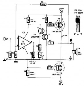
This audio power amplifier employs two complementary MOSFETs (IRF9520 and IRF520) to provide up to 20W output into an 8-ohm speaker. A TL071 operational amplifier functions as the input amplifier. The MOSFETs require heatsinking with a thermal resistance of...
This project is finalized, that means it is no longer experimental. This amplifier, although limited in output power (20W), has been designed to give the best listening pleasure. No compromise has been made during components choice: the 845 output...

This circuit is a 20W Audio Amplifier kit, based on the TDA2005 IC, a class B dual audio amplifier, specifically designed for car radio applications etc. Power supply - 18 VDC. Output power - 20 W, 4 ?. IC...
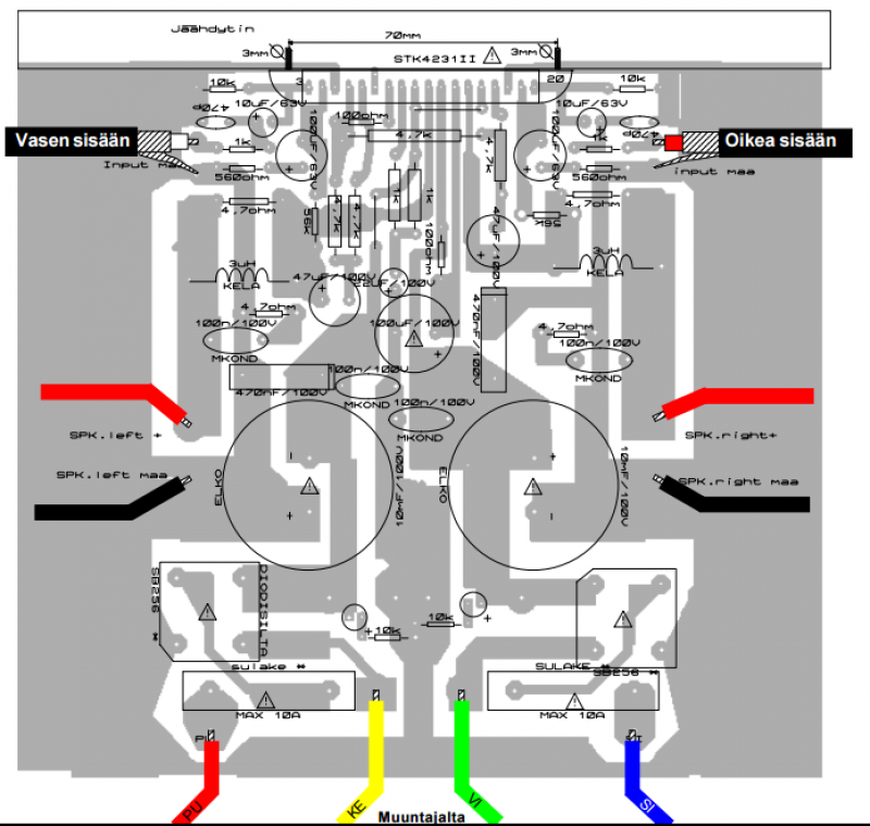
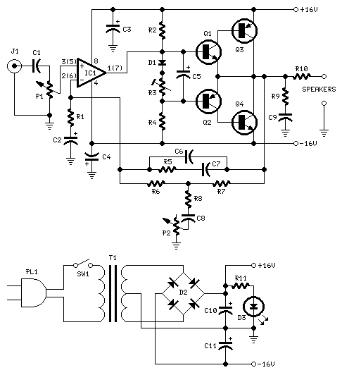
This amplifier is of such high quality that it would be an understatement to call it a HIFI amplifier. According to HIFI-confirmed-Finland, the frequency response must be direct and distortion <1% 20-20 kHz. Our power amplifier circuit meets the above requirements for bandwidth 5Hz - 500 kHz, however, the frequency band is limited to prevent interference. The amplifier meets the requirements for a reference amplifier, which is suitable for measurement and comparison operations. Small 12-24V voltage system amplifiers operating in the power and properties are somewhat modest, for instance, testing decent speakers. The amplifier is also suitable for demanding PA use. When music occurs at shallow close 20Hz sound levels, the whole amplifier power reserve may need to be temporarily used. This happens especially when the low-frequency emphasis equalizer or amplifier is used, for example, TV. Watching a movie with lots of sound effects, if the power is not enough in that situation, the sound from the speakers is distorted, reducing the enjoyment of hearing or even damaging the speaker drivers. The distortion of human hearing range is only about 20 Hz-20 kHz. The hi-fi speaker gamut extends at its best to 25kHz and the hearing area of bats "remains" at 150 kHz, so what are the practical benefits of the amplifier's superior frequency characteristics? The power of less than 1% distortion mentioned in the title 220W blue means the so-called total maximum amount of distortion. This includes TIM distortion (Transient intermodulation) as well as IM-distortion (intermodulation-distortion). TIM distortion occurs in connection with high-speed percussion sounds, such as the sound of dishes on drums. If the amplifier's share of this distortion is high, the amplifier will not be able to play the sound clean, but the sound will be distorted. The higher the frequencies the amplifier is capable of playing, the less is TIM distortion. If the amplifier would be able to repeat 600 kHz, distortion would not occur at all. IM distortion means that the amplifier generates excess denominated, the so-called undesirable ghost signals. For example, fed in to 19 kHz. And 20 kHz, consists of the difference between 1kHz. Safety Because this amplifier has AC parts, its construction is permitted only in the technical work of teachers. Even in this case, the device should be checked by experts before connecting it to the network. Although the equipment has been revised, it is worth remembering that even the only speaker outputs may at best affect almost 70V the effective voltage. Therefore, caution is necessary during building and operation. For instance, the speaker terminals should be protected against contact. Building instructions and testing of the amplifier circuit board components will be worth and an amplifier solder test in three stages: 1) The components of the power side, and all the cables signal cables except installed 2) any other circuit board components plus not only hybrid circuit STK 4231 3) STK 4231 placed and cooled, and the input signals the wires connected. Installation of the power-side components and testing should be done carefully. The transformer wires insulation must first be removed carefully or checked that this has already been done. Then the transformer conductors order is checked on the transformer side. The circuit board parts include STK4231II Hybrid, Led green, resistors of different values, ceramic and plastic capacitors, a rectifier, fuse holders and fuses, a coil, line voltage parts, potentiometer, RCA connectors, speaker output screws, and a cooling unit.