
555 point-frequency TV terminal circuit

This circuit is designed to process signals for various applications, particularly in communication systems. The input circuit serves as the initial stage for signal conditioning, where the input attenuator RP1 adjusts the signal level to a suitable range for further processing. The emitter follower VT1 acts as a buffer, providing high input impedance and low output impedance, ensuring minimal loading on the preceding stage while driving subsequent components effectively.
The line frequency synchronization generator is crucial for maintaining timing accuracy within the system. It generates a stable reference frequency that is used to synchronize the operation of the other circuit elements. This synchronization is essential for ensuring that the sample-and-hold circuit accurately captures the input signal at the correct times, thereby enhancing the fidelity of the processed output.
The sample-and-hold circuit temporarily holds the sampled signal, allowing for stable processing and conversion. This stage is vital in applications where the signal needs to be digitized or modulated, as it ensures that variations in the input signal do not affect the output performance.
The voltage control delay generator introduces a delay in the signal path, which can be adjusted based on the control voltage. This feature is beneficial for phase modulation and other applications where precise timing is essential. The RF modulator at the output stage converts the processed signal into a radio frequency signal suitable for transmission.
Overall, the integration of these components allows for a versatile and efficient circuit capable of handling various signal processing tasks, making it a valuable design in modern electronic systems.As the figure 14-17 shows, this circuit is composed of the input circuit, the line frequency synchronization generator, the sample-and-hold circuit, the voltage control delay generator and the RF modulator.The input circuit is composed of the input attenuator RP1 and the emitter follower VT1. The astable multivibrator is composed of the IC2 and RP2,.. 🔗 External reference
Related Circuits
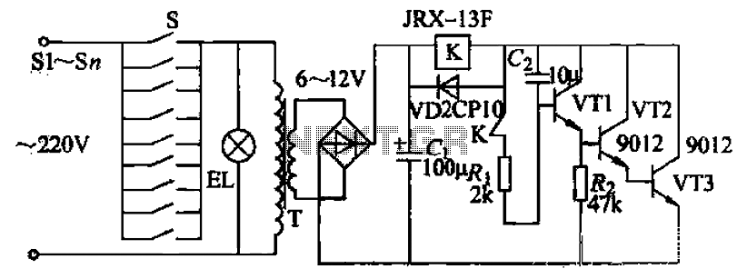
Pressing the button switch Sl-Sn activates the circuit, turning on the transformer T. The low-voltage alternating current from the secondary winding is directed to a bridge rectifier and a filter capacitor Ci, which produces a DC voltage. This voltage...
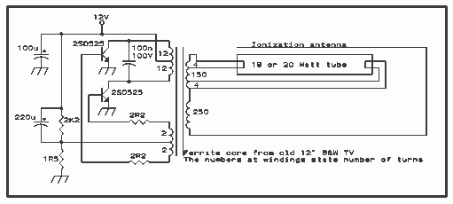
Here is the schematic diagram for a 20 Watt driver. I developed this circuit in 1985, and used it to build a lamp that found much use both as camping light and as emergency light during the then-frequent power...
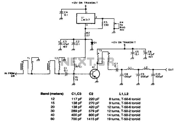
This linear amplifier provides a 10-W PEP output with a 1.25-W drive on the 10 m band. The transformers, T1, T2, and T3, consist of 10 turns of bifilar windings on an FT-50-43 toroidal core and are designed for...
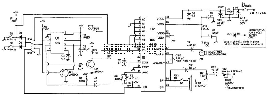
The circuit utilizes an ISD1016 audio record/playback chip from Information Storage Devices, Inc. to record and playback messages on demand. While it is primarily designed for use with transmitters, it can also serve as an electronic notepad or similar...
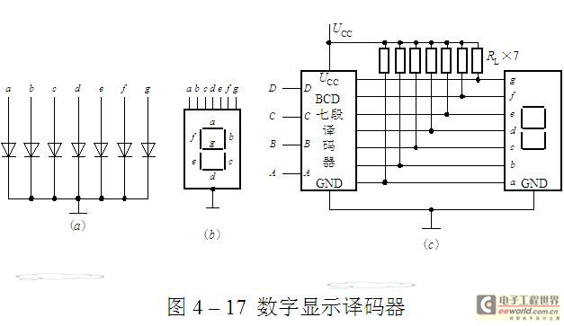
The luminescent diode (LED) is constructed from gallium arsenide (GaAs), a specialized semiconductor material, and gallium arsenide phosphide. It can be used individually or assembled into segment-type or lattice LED display devices. The display unit consists of a sectional...
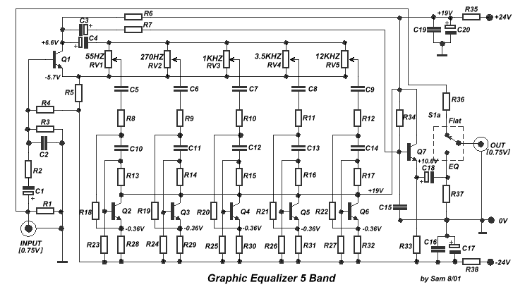
Another unit of graphic equalizer with five bands. The primary distinction from other circuits is the use of transistors instead of integrated circuits (ICs), and the power supply operates at +/- 24V DC, which ensures low distortion and greater...