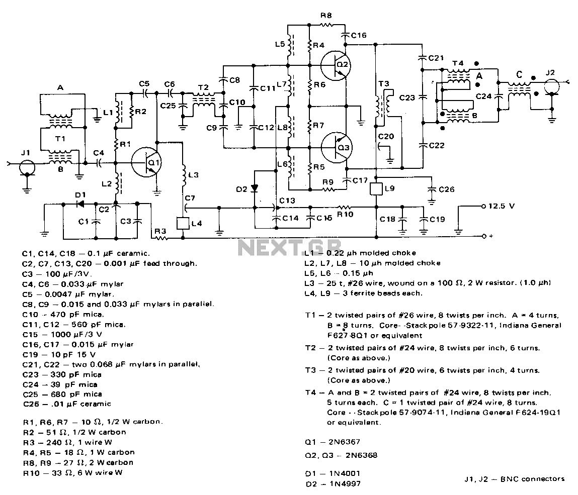
80W-3-30mhz-amplifier

This amplifier employs a 2N6367 transistor as a driver along with a pair of 2N6368 transistors. The 2N6367 is rated for a maximum output of 9 W (PEP) and is required to deliver 5 W (PEP) at 30 MHz, achieving an intermodulation distortion (IMD) performance of approximately -37 to -38 dB. At lower frequencies, the drive requirements decrease to the range of 2-3 W (PEP), resulting in improved IMD performance of better than 40 dB. The final stage of the transmitter design utilizes two 2N6368 transistors in a push-pull configuration, each rated for 40 W (PEP) with a maximum IMD of -30 dB, although a typical performance of -35 dB is observed for narrowband operation. In the absence of frequency compensation, the amplifier can produce 90 W (PEP) within the 25-30 MHz band, maintaining an IMD performance of -30 dB. If only the power amplifier stage is frequency compensated, it can achieve 95 W (PEP) at frequencies between 6-10 MHz.
The amplifier circuit described integrates a driver stage and a final output stage, utilizing specific transistor models to achieve desired performance metrics. The 2N6367 transistor functions as the driver, providing the necessary gain and output power to drive the final stage. Operating at 30 MHz, the driver must produce 5 W (PEP) while maintaining acceptable intermodulation distortion levels. The design ensures that at lower frequencies, the power requirements are reduced, allowing for enhanced linearity and reduced distortion.
The final amplification stage comprises two 2N6368 transistors configured in a push-pull arrangement. This configuration is advantageous for improving efficiency and linearity, as it allows for the cancellation of even-order harmonics, thereby enhancing the overall performance of the amplifier. Each 2N6368 transistor is capable of delivering up to 40 W (PEP), and the expected IMD performance is typically around -35 dB for narrowband applications, indicating a high-quality output signal.
Without implementing frequency compensation, the amplifier can achieve a significant output power of 90 W (PEP) in the 25-30 MHz range, though this comes with a trade-off in distortion performance. The design can be optimized further by applying frequency compensation to the power amplifier stage, which permits an output power of 95 W (PEP) at lower frequencies (6-10 MHz). This highlights the flexibility of the amplifier design to cater to various frequency bands while maintaining robust performance characteristics.
Overall, the described amplifier circuit combines effective transistor selection with strategic circuit design to deliver high output power and low distortion across a range of frequencies, making it suitable for various RF applications.This amplifier utilizes a 2N6367 and a pair of 2N6368 transistors. The 2N6367 transistor is employed as a driver and is specified for up to 9 W (PEP) output. In the amplifier design the driver must supply on 5 W (PEP) at 30 MHz with a resulting !MD performance of about -37 to -38 dB. At lower operating frequencies, drive requirements drop to the 2-3 W (PEP) range and !MD performance improves to better than 40 dB.
Two 2N6368 transistors are employed in the final stage of the transmitter design in a push-pull configuration. These devices are rated at 40 W (PEP) and -30 dB maximum !MD, although -35 dB performance is more typical for narrowband operation.
Without frequency compensation, the completed amplifier can deliver 90 W (PEP) in the 25-30 MHz band with !MD performance down -30 dB. If only the power amplifier stage is frequency compensated, 95 W (PEP) can be obtained at 6-10 MHz.