
A common emitter amplifier

The common emitter amplifier circuit is characterized by its ability to provide significant voltage gain, making it a fundamental building block in analog electronics. The transistor, functioning as the active component, is typically an NPN type for this configuration. The input signal is fed into the base terminal, where it modulates the current flowing from the collector to the emitter. This modulation results in an amplified output signal at the collector terminal, which is inverted in phase relative to the input signal.
The resistors in the circuit play critical roles in biasing the transistor and setting the operating point, which is essential for linear amplification. The resistor R1 is responsible for establishing the base current, while the emitter resistor Re serves to stabilize the operating point against variations in temperature and transistor parameters. The coupling capacitors ensure that only AC signals are passed to the next stage of the circuit, effectively blocking any DC offset that might affect performance.
The load resistor RL is crucial for determining the output impedance of the amplifier. By selecting appropriate values for R1, Re, and RL, the designer can optimize the amplifier's gain, bandwidth, and input/output impedance characteristics. The overall performance of the common emitter amplifier can be assessed through parameters such as voltage gain (Av), input resistance (Rin), and output resistance (Rout), which are influenced by the chosen resistor values and the transistor's characteristics.
In summary, the common emitter amplifier is a versatile and widely used circuit configuration in electronic design, providing essential functionality in various applications, including audio amplification, signal processing, and more complex integrated circuits. Its design requires careful consideration of component values to achieve the desired performance metrics while ensuring stability and reliability.A common emitter amplifier (1) Total pole amplification circuit structure and key emitting device common emitter amplifier circuit refers to the emitter (e) of the input signal and the output signal of the common ground of basic amplifier circuits. The circuit of l-l basic structure as shown in the figure, its key components include a transistor, four resistors and two capacitors. Where the circuit bias resistor R 1 and friends through the power supply to the base of the transistor (b) power supply; a load resistor Re is given by the power transistor collector (c) power supply; two capacitors are played through AC DC blocking effect coupling capacitor; a resistor RL is the output signal carrying the load resistor.
NPN type transistor amplifier with PhrP biggest difference is that the power supply: The NPN transistor amplifiers, power supply is fed to the positive supply transistor collector (c); a PNP transistor amplifier, power supply is sent to the negative supply the transistor collector electrode (c). Input signal is applied to the transistor base (b) and between the emitter (e), and the output signal is the collector of the transistor (c) and from electrode (e) between the transmitter, shows an emitter (e ) for the input signal and the output signal common terminal, thus said common emitter transistor amplifier, commonly used in the transistor voltage amplification circuit.
Related Circuits
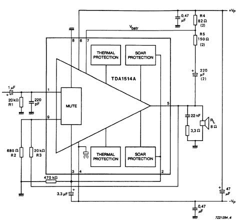
The TDA1514 audio amplifier circuit design is an electronic project capable of delivering high audio power output using a specialized audio integrated circuit (IC) and a few common components. Manufactured by Philips Semiconductor, the TDA1514 audio IC can provide...
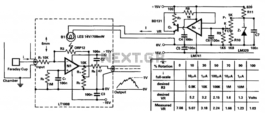
To amplify small current signals, such as those from an electron collector inside a vacuum chamber, it is beneficial for reasons related to noise and bandwidth to utilize a "head amplifier" connected to the chamber. The operational amplifier N1...
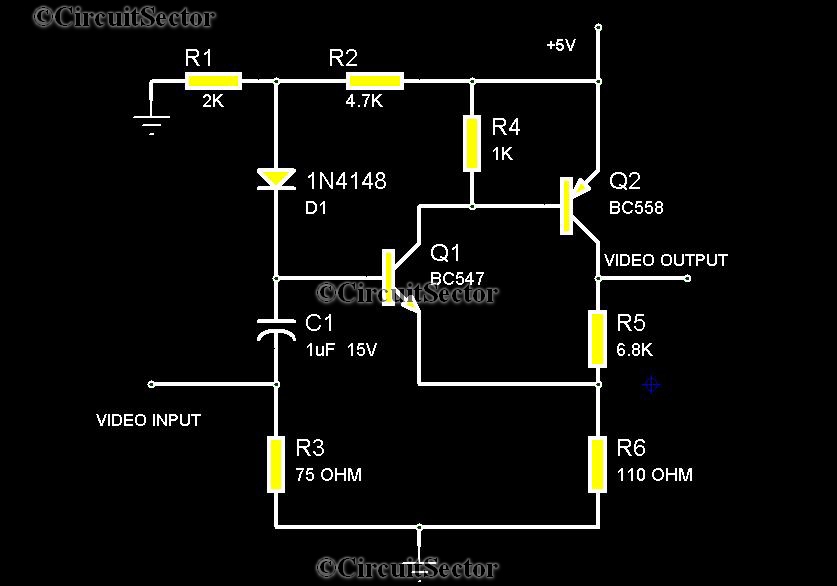
There are instances when it is necessary to view video clips captured by a digital camera on a television. This can be accomplished by connecting the camera's video output to the television's video input. However, a direct connection is...

This differential amplifier utilizes a CA3193 BiMOS operational amplifier. It serves as a classical differential input-to-signal-ended output converter, which, when paired with a low-resistance signal source, will sustain a high common-mode rejection ratio (CMRR), provided that R1 equals R3...
If you want to test an amplifier, a dummy load may be more convenient for speakers to use than actual speakers, due to noise or damage to the speakers. This circuit behaves in terms of impedance and frequency response...
The 2SK2975 has reportedly been discontinued by the manufacturer, with the RD07MVS1 from Mitsubishi serving as its replacement. This new device is very similar but appears to have slightly higher gain—10 dB typical at 520 MHz compared to 8.4...