
About Area 50

This circuit operates as a frequency divider, utilizing a 10 MHz reference signal to generate lower frequency outputs. The choice of output frequencies—1, 10, 100, and 1000 Hz—allows for versatile applications in timing and clock generation. The use of jumpers to select pulse width adds flexibility, enabling customization based on specific requirements. The synchronization feature is crucial for applications requiring precise timing alignment, particularly in systems interfacing with GPS or other timing sources.
The outputs at pins 8 and 9 of the 7474 flip-flop are the result of the division process. The 7474 is a dual D-type flip-flop that can be configured for various counting and timing applications. The circuit design allows for easy interfacing with other digital components or systems.
The input section's depiction as a sine-to-square converter suggests that the circuit can accept analog signals and convert them into a digital format suitable for processing by the flip-flop. While the prototype does not include the specific components for this conversion, it is common practice to use a logic-level signal directly at pin 5 of the 7474. This simplifies the design and reduces component count.
For applications where input signals are analog, employing a line receiver can effectively square up a sine wave, ensuring that the input to the flip-flop is clean and reliable. This approach enhances the performance of the circuit, particularly in environments where signal integrity is paramount. Overall, this frequency divider circuit is a robust solution for generating accurate timing signals across a range of applications.This circuit divides a 10 MHz reference to 1, 10, 100 or 1000 pulses per second. The pulse width is also jumper selectable with lots of choices. A sync input will align the pulses with an external pulse, say from a GPS receiver. The outputs are hiding over there at pins 8 and 9 of the `7474. The input is at the bottom of the schematic and is reall y just a sketch of a typical sine-to-square converter. Those parts aren`t on the prototype in the photo. Just use a logic level directly into pin 5. A line receiver is a good way to square up a sine wave, too. 🔗 External reference
Related Circuits
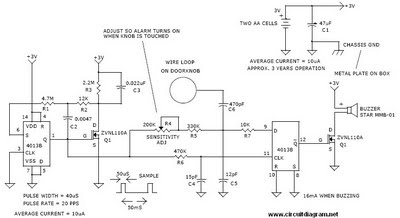
This is a door knob touch alarm designed for home security purposes. The alarm will activate when someone touches the metal door knob. This circuit will not function on a fully metal door. Currently, circular batteries are used, but...
Inquiry regarding the possibility of connecting two dimmers in series to achieve precise control over the light emitted by a bulb. The objective is to attain medium to high precision in light emission for a school project. Additionally, there...
The mine railway connects the national railways and intermediate links of the mining area, serving as an important component of the railway transport network. Statistics indicate that the Chinese mine railway extends over 20,000 kilometers, with numerous road junctions...
The Controller Area Network (CAN) data rate ranges from 10 kbit/s to 1 Mbit/s, with recommended distances of 40 to 1000 meters using two twisted pairs—one for data and the other for power and ground. Up to 110 nodes...
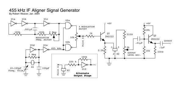
The resonator appears to be highly susceptible to harmonics. For instance, if the resonator frequency is set at 455 kHz, it also permits frequencies at 910 Hz, 1820 kHz, and 3.640 MHz, which seems to be dominant. Frequencies around...
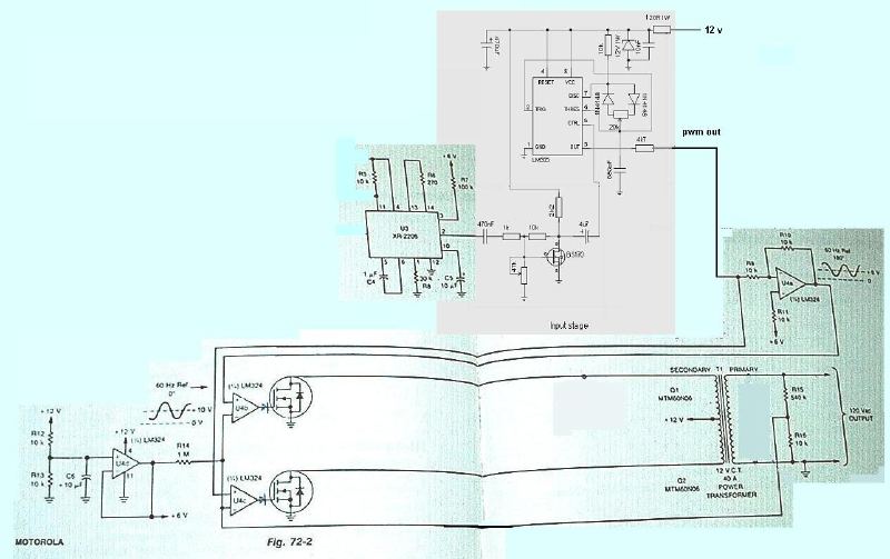
A few months ago, a search was conducted for an easy-to-build PWM inverter that does not require any PIC programming. The investigation led to a consideration of a 555 PWM amplifier circuit. The 555 timer IC is widely used in...