
Adopt the two-dimentional bar-code scanner of DSP56F826 chip to introduce systematically

The system architecture integrates several key components and processes to ensure efficient operation and high-quality data capture for two-dimensional barcode scanning applications. The DSP56F826 chip plays a central role in processing the data captured by the OV7120 image sensor, which is designed to operate efficiently within the specified resolution and speed parameters. The RS-232 communication interface facilitates real-time data transfer to a computer, allowing for immediate processing and display of the captured barcode information. The use of external SRAM enhances the system's data handling capabilities, enabling the storage of image data prior to processing. The error correction mechanism is robust, ensuring high data integrity during transmission, which is critical for applications requiring reliable barcode scanning. The overall design emphasizes a balance between performance and cost, making it suitable for various applications in the field of barcode scanning and data acquisition.The system regards DSP56F826 chip as the key control module, uses the sensory chip of CMOS digital image, reachable 640* 480 picture element of definition that the picture is gathered. When needing the vision which carries on the high-resolution to be gathered, can use the chip cost will thereupon increase of 1024* 1024 picture element instead.
D ecipher reliability is high. The bit error rate got at present does not exceed 1/60, 000, and is updating, expect the bit error rate not to exceed 1/20 million. Adopt RS-232 communication interface, upload the two-dimentional bar code information obtained to the display processing of the computer in real time.
The grade of error correction reaches 8 grades, correction capability is strong. Two-dimentional bar-code scanner system block diagram such as Fig. 1 Shown. The sensory chip of CMOS picture is a photoelectric transition element, use and gather the two-dimentional bar code picture, direct output is a digital signal. Expanded SRAM by the outside and stored this data, and then send DSP, carry on image manipulation, one yard of word division, one yard of word recognition, signal error correction, etc.
, after the recognition of a series of two-dimentional bar code information is finished, serve the I/O interface of program control and provide and stop applying for signals, DSP responds to this and stops applying, enters the interrupt service routine. The two-dimentional bar code data after the decipher are conveyed from I/O mouth to the computer by SCI RS-232, and reveal on the screen.
Software program and PDF417 codebook are all stored in FLASH in DSP chip, and the two-dimentional bar code image data gathered dynamically is stored in SRAM. The system hardware circuit is mainly composed of seven parts: The bar code vision is gathered the circuit, circuit, expansion circuit of the memorizer of DSP top management, exporting the interface circuit, resetting with clock circuit, power controlling circuit, lighting controlling circuit.
This circuit regards sensory chip of OV7120 black-and-white image as the core, the definition of this chip reaches 640* 480 picture element, the imaging speed is frames per second 30, take the non-interlaced scanning mode, output it as the digital signal. The low power dissipation of this chip, the price is cheap, though CCD chip is superior to CMOS chip in such aspects as signal to noise ratio, degree of sensitivity, imaging quality, but in this system design, it is comparatively suitable to adopt CMOS chip.
The bar code picture is gathered the circuit Fig. 2 China, Y0-Y7 is the digital output of bus line, HREF is a horizontal reference signal, namely the scanning signal of walking; VSYN is a vertical sync signal, namely field synchronizing signal. PCLK exports for the picture element clock. This circuit uses 5V direct current, is offered by controlling circuit of the power. Though chip this use the intersection of 5V and working voltage, it offer the intersection of I/O and mouth of 3.
3V, so it can link with I/O voltage directly for DSP of 3. 3V, do not need level switch. When DSP receives VSYN signal, show the chip begins to gather the first frame bar code image data, receive HREF signal subsequently, the chip starts first lines of data acquisition, want a PCLK signal each time, gathers a signal that picture element is lighted with chip, as DSP receives the next HREF signal, the chip carries on second lines of data acquisition, until finishing gathering 640 lines of data, the chip stops gathering. When DSP receives the next VSYN signal, show that gathers the data of the next frame with chip. As shown in Fig. 1, this circuit regards DSP56F826 as the core. When the sensory chip of OV7120 picture plans to gather the image data of bar code, DSP sends out an initialization signal, control SRAM redistribution address block, the sensory chip of the picture begins to gather the image data of bar cod
🔗 External reference
Related Circuits
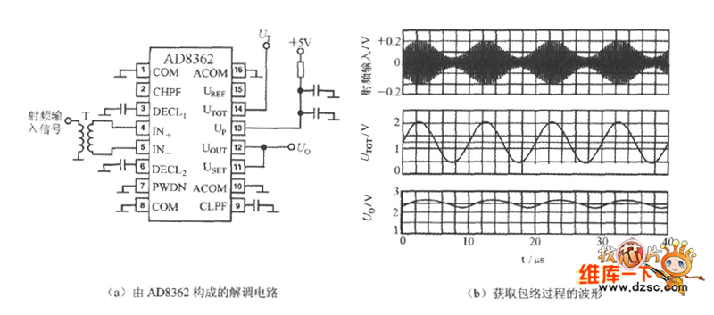
The UTGT side of the AD8362 can be utilized to create a demodulation circuit. It extracts the envelope from the RF amplitude and converts it into a low and mid-frequency signal prior to demodulation. The waveforms associated with the...

The figure utilizes a controller as the primary equipment for gathering and controlling digital data within an on-site monitoring system. The stability of on-site control operations is crucial to the overall system performance. Therefore, a simple and stable structure...
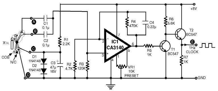
1Hz Clock Generator Circuit with Chip On Board (COB). The COBs used in different watches may differ somewhat in their configuration. However, through trial and error, one can identify the appropriate points corresponding to points A, B, C, and...
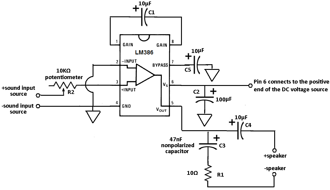
Terminals 1 and 8 serve as the gain control for the amplifier. Adjustments to the gain can be made by connecting a resistor and capacitor, or just a capacitor, between these terminals. In this circuit, a 10 µF capacitor...

The circuit described uses a single chip, IC BA3812L, to realize a 5 band graphic equalizer intended for use in hi-fi audio systems. The BA3812L is a five-point graphic equalizer that integrates all the necessary functions onto one IC. The...
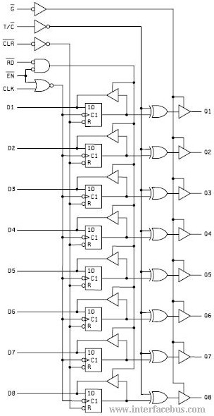
The 74ALS996 component is designed for the commercial temperature range, while the 54ALS996 is available for operation within the military temperature range. Although both components are typically offered in the same package styles, this may change as the usage...