
ADum3223 issue (H bridge)
")
The circuit utilizes a Zener diode for voltage clamping, providing a protective measure against over-voltage conditions that could potentially damage sensitive components like the ADuM3223. The implementation of the Zener diode should be strategically placed across VDDA to shunt excess voltage away from the IC. The design must consider the maximum voltage ratings of all components to ensure reliability under transient conditions.
In the H-bridge configuration, the placement of the ADuM3223 gate drivers is crucial. When employing two separate drivers for the upper and lower sides, it is advisable to keep the outputs on opposite legs to maintain symmetrical operation and minimize cross-talk. This arrangement not only simplifies the logic but also ensures that the gate drivers can effectively manage the switching without interference.
The use of R3 and R4 resistors is a smart design choice, as they assist in maintaining the voltage levels necessary for the gate drivers to operate correctly. However, careful consideration must be given to their values and the overall bus voltage to avoid excessive power dissipation. The start-up sequence must be adhered to, ensuring that the low-side MOSFETs are activated first to allow for proper bootstrap charging of the high-side drivers.
In conclusion, the proposed circuit modifications and layout adjustments should enhance the performance and reliability of the H-bridge configuration. Continuous monitoring of the output signals during operation will aid in identifying any further discrepancies, and adjustments should be made based on empirical data gathered from testing.Zender diode to do the over-voltage protection, this issue might be solved. Am I right or I need to do another thing to protect it. Please give me any advice. A zener diode will help if over-voltage on VDDA if that is the cause of the failure, but with a 12V rail, it would take a lot of ringing to cause an over-voltage failure on the ADuM3223. The part can withstand 20V, so the ringing would have to be almost 50% of your voltage rail. Is there a chance you have an oscilloscope probe ground on GNDA If a non-isolated, non-differential probe ground is placed on GNDA, a short can be created between GNDA and GNDB. I would probe the VIA and VIB commands to see if there is a mismatch between the two sides of the H bridge, and try to figure out what the difference is between the two sides.
Thanks for your advice, After probing the VIA, VIB, VOA, VOB, the signal is fine in input(VI) and output(VO) when mos doesn`t be connected, but if the mos is connected, the burn out side`s output signal`s high level is only 1/2 supply voltage. We think it might because the PCB is old version and it isn`t designed for Adum3223, so we decide re-layout the PCB and will follow the ADI`s CN0196 recommendation circuit like the following circuit.
Could you help me check does it follow your guide line By the way, from CN0196, one Adum3223 drive half bridge, but if I use one adum3223 drives upper side H-bridge and the other one drivers down side H-bridge, is any different or concern between these two way I believe the application note put the outputs of the gate drivers on opposite legs of the H bridge to simplify the input on each chip. The application note allows for high-side supply charging, even when not switched, but for your first circuit, as long as a minimum duty cycle and frequency is maintained, the VDDA on both chips will have sufficient voltage.
2)The high side gate driver doesn`t break immediately, normally it`s can run around couple minutes(with loading) in 500Hz(the max frequency is 1MHz) but eventually the IC would die(It only breaks when the gate driver drivers the Mosfet and loading, If without loading, the function is no problem). 3)Yes, the gate driver works well in no bus voltage but with Mosfet. This condition that the output only 1/2 supply is happened after the gate driver breaks and we try change the circuit and add more element to fix it.
In the first time, the gate driver works well in with Mosfet or without. The situation that gate driver breaks is in the beginning, After I change the circuit, I didn`t put the loading in the H-bridge because of the wrong level in output. We still don`t figure out where is wrong and the circuit difference between two side half bridge, it why we decides to re-layout and wish this version can put all risks in to account to fix it.
The benefit of the R3 and R4 resistors in the CN0196 design is that when all the MOSFETs are off, the highside grounds are pulled low, charging the VDDA`s. There is a tradeoff in power with higher bus voltages, since when the high-side switch is on, the bus voltage is applied to R3 or R4.
For higher voltage designs, R3 and R4 are not recommended, but the start-up sequence for the system should have the low side switches turn on before the high side switches (in order to charge the high sides through the bootstraps). Does the circuit only fail at higher frequencies There is an upper limit to how fast these gate drivers can be driven, which comes from the power dissipation in the part.
The ADuM3223 datasheet states a 1 🔗 External reference
Related Circuits
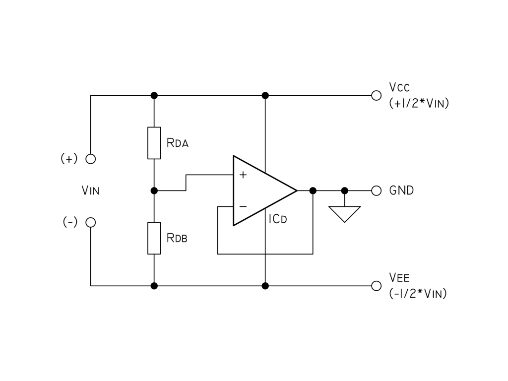
To eliminate noise, a 100µF capacitor and a 100nF bypass capacitor are used across the supply, along with two 10nF capacitors in parallel with the resistors Rda and Rdb (each 10K). For current limiting, a 22K resistor is paralleled...
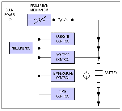
Application note on designing linear and switch-mode (switching DC-DC converter current source) battery charger applications that require external microcontrollers and related system-level issues for notebook computers. The application note provides guidance on the design of both linear and switching DC-DC...
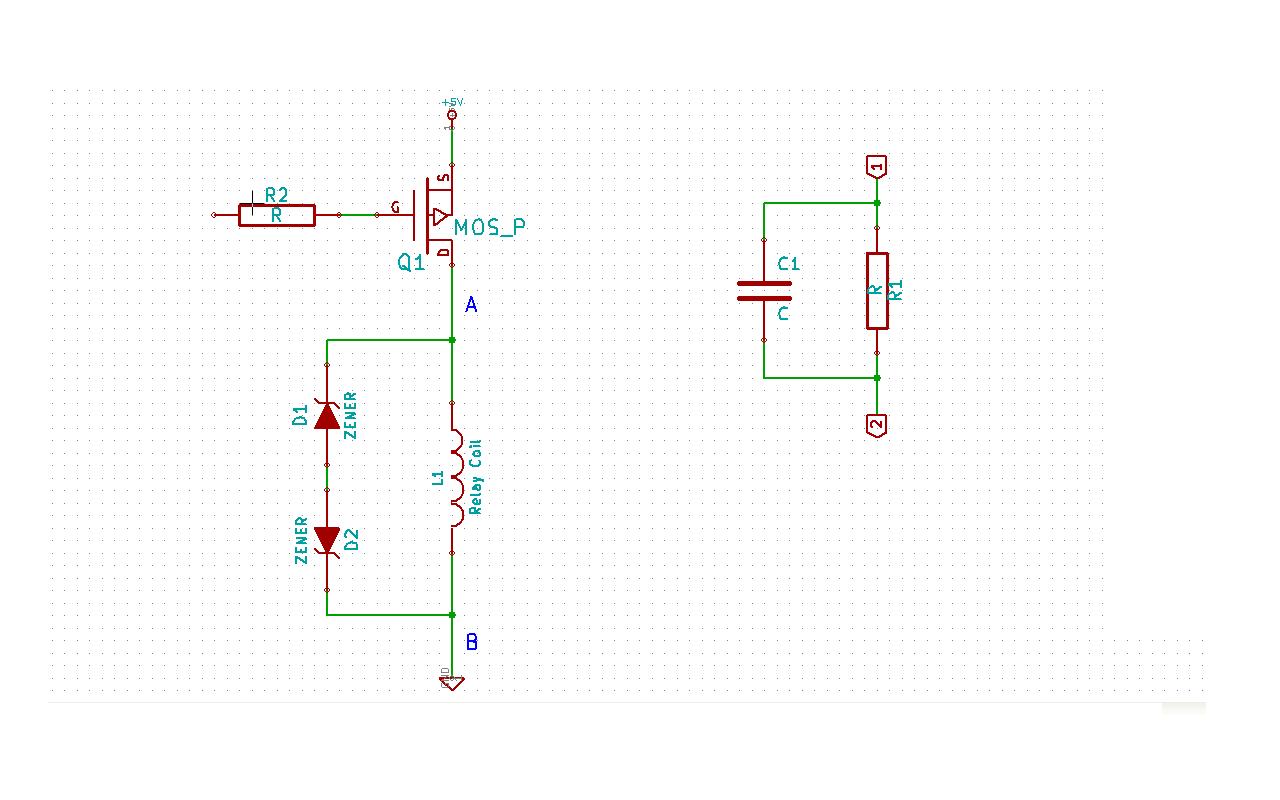
Although this may be a basic question, there is still some struggle with it. In this schematic, two zener diodes D1 and D2 are connected back-to-back across relay coil L1. The breakdown voltage (BVds) is -30V for Q1. The...
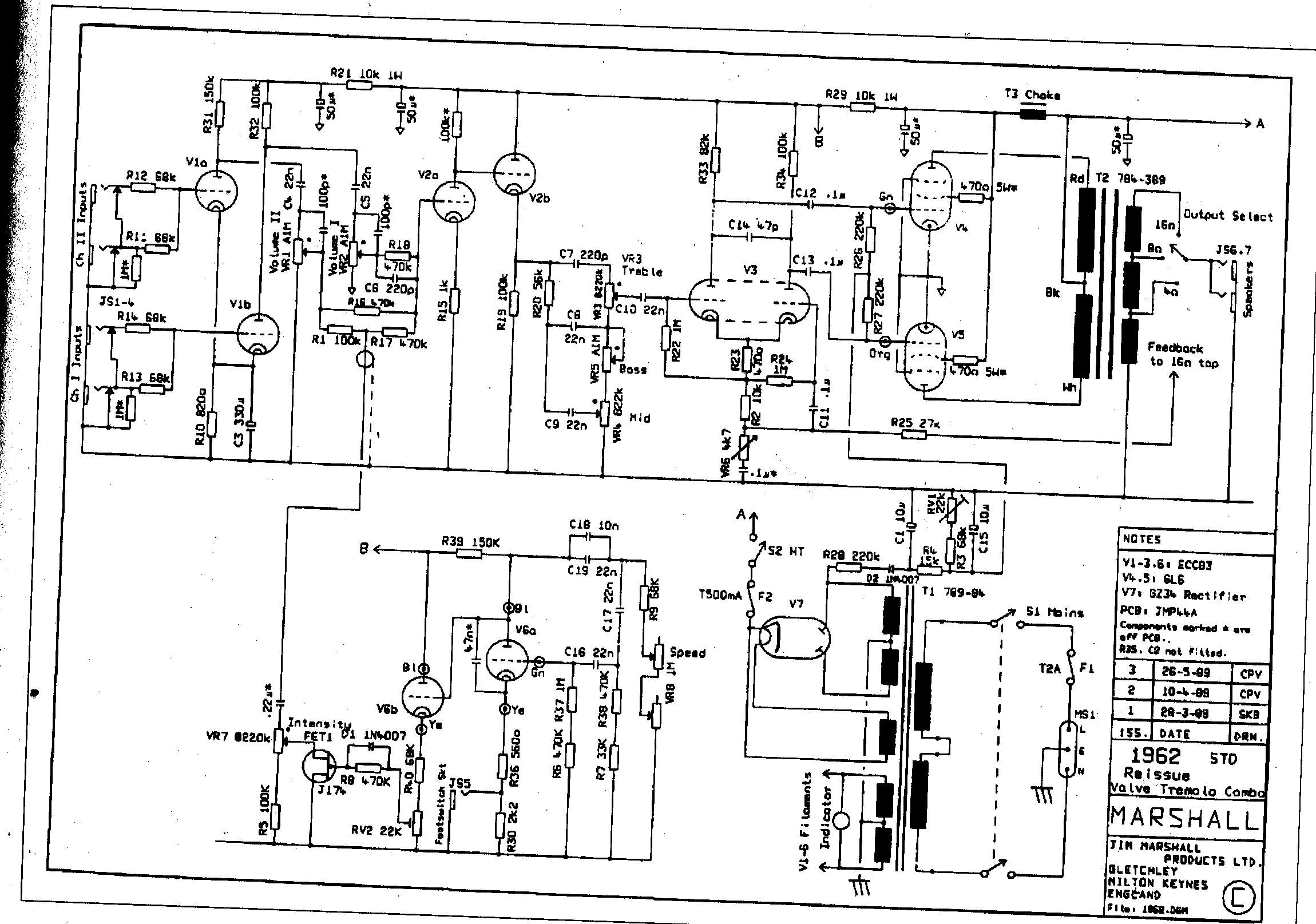
The Sovtek 5881 tubes included in these amplifiers are low-quality and produce a corresponding sound. It is advisable to replace all tubes with a Sovtek GZ34, Valve Art or GT KT66 tubes, and Ei Gold preamp tubes. The KT66...
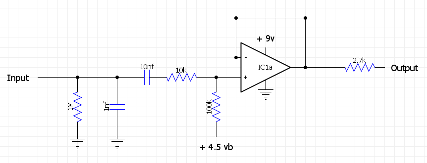
Currently, there is a prototype of a guitar pedal in development. There are issues with the input buffer, and assistance is needed to address these problems. The input buffer in a guitar pedal is a critical component that serves to...
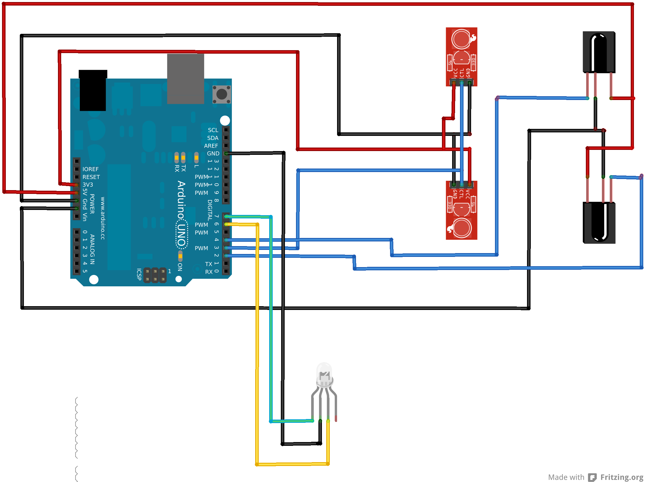
An Arduino Uno is connected to two infrared (IR) transmitters and their respective receivers. When one of the receivers detects a beam break, a strand of LEDs displays a pattern. While this setup functions correctly in principle, an issue...