
An Intel 8088 Maximum Mode Single Board Computer System

The first page includes the schematic of the CPU section, which features the 8088 microprocessor, an 8284 clock generator, an 8288 bus controller, and address and data line buffers. The 8284 is essential for generating clock, ready, and reset signals. The 8088 can be placed into a non-ready state by grounding either of the RDY inputs on the 8284. Figure 3 illustrates the schematic diagram of the CPU module. The 8288 is utilized to decode the status outputs of the 8088, as the microprocessor operates in maximum mode. In addition to generating memory and I/O port read/write signals, the 8288 controls the bidirectional data bus driver (the 8286) and the lower address latch chip (the 8282). Since the upper address lines are not multiplexed, they only require buffering, which is achieved through the use of the LS244 octal buffer. Buffering the address and data lines is crucial for any potential future expansion of system memory or I/O spaces. While the 8088 can drive a limited number of TTL loads directly, the drivers enhance its capability to manage a significantly higher load. Figure 3 depicts the schematic of the CPU module.
The second page of schematics outlines the MEMORY section, which consists of 8K bytes of RAM and 8K bytes of EPROM. The EPROM utilized is a 2764 type. Address lines A0 through A12 are employed to select one of the 8192 locations within the EPROM. The data lines are activated when both enable signals are low. The OE signal is managed by the system's MRDC signal (memory read command), while the CS signal is low when address lines A13, A14, and A15 are all high (via output 7 of the LS138). This addressing scheme provides an address range for the EPROM from E000 to FFFF, necessitating its placement in high memory due to the power-on instruction fetch sequence. Figure 4 illustrates the schematic diagram of the MEMORY module. The 6264 RAM operates similarly, with the exception of the inclusion of the MWTC (memory write command) signal and the connection between CS and output 0 of the LS138, which activates when the address bus is in the range of 0000 to 1FFF. The LS138 offers six additional outputs for mapping 8K sections into the initial segment.
The third page of schematics presents the I/O section, which provides 24 parallel I/O lines and a serial I/O line. The LS138 is employed to map out eight distinct I/O port areas, with the first at address 00 and the eighth at E0. These port addresses correspond to the states of address lines A5, A6, and A7. Port-bank 00 manages the analog section circuitry, while port-bank 20 is designated for the 8255, which generates 24 parallel I/O lines, and bank 40 is allocated for the 8251 serial chip. Both peripherals (the 8255 and the 8251) are connected to the data bus and utilize the I/O read/write command signals IORC and IOWC. For the 8255, two address lines (A0 and A1) are used to access the internal circuitry, whereas the 8251 requires only one address line (A0) for control. The BAUD rate is regulated by the software utilized to initialize the 8251, ensuring effective communication through the serial interface.
This comprehensive design showcases the integration of essential components to create a functional single-board microcomputer system, providing a valuable educational experience for students in the field of computer science.As an integral part of an advanced computer science course in microcomputer systems it was thought that students could benefit from the design of a single board computer system based on a readily available microprocessor. This led to the project that is described in this paper. Most of the actual design work was done by James Antonakos as part of an Independent Study project. The result was a single board microcomputer system (SBMCS) that requires only a power supply and a serial monitor to be fully functional. This same project will be assigned to advanced undergraduate and intermediate graduate computer science students working in teams.
A photograph of the working single board microcomputer system that was designed and constructed is given in Figure 1. The purpose of this document is to briefly describe the theory of operation behind the 8088 Single Board Microcomputer.
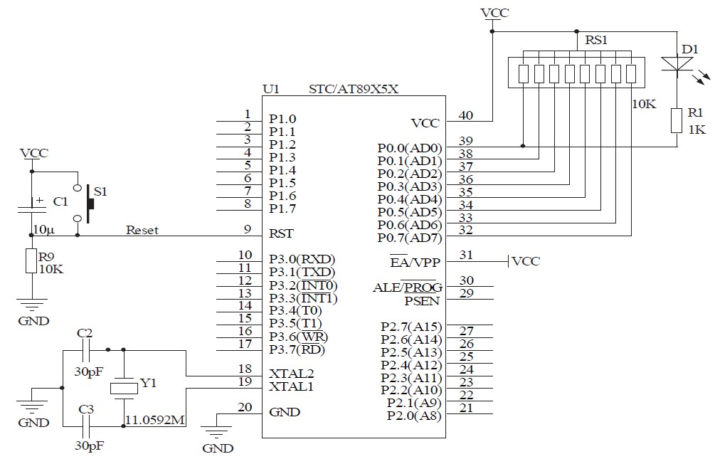
The system has been designed to meet the following requirements: The descriptions that follow are based on the 4-page schematic for the system. Page one is the schematic of the CPU section, containing the 8088, an 8284 clock generator, an 8288 bus controller and address and data line buffers.
The 8284 is needed to generate the clock, ready and reset signals. The 8088 may be placed into a non-ready state by grounding either of the RDY inputs on the 8284. Figure 3 shows the schematic diagram of the CPU module. The 8288 is needed to decode the 8088`s status outputs since we are operating the 8088 in maximum mode. In addition to generating the memory and io-port read/write signals the 8288 also controls the bidirectional data bus driver (the 8286) and the lower address latch chip (the 8282).
Since the upper address lines are not multiplexed all we need to do is buffer them, hence the use of the LS244 octal buffer. Buffering the address and data lines is very important if future expansion of the system memory or i/o spaces is desired.
By itself the 8088 is able to drive a few TTL loads but the drivers provide it with the ability to drive many more loads. Figure 3 shows the schematic of the CPU module The second page of schematics is the MEMORY section. This section contains 8K bytes of RAM and 8K bytes of EPROM. The EPROM used is a 2764. Address lines A0 through A12 are used to select one of 8192 locations inside the EPROM. Its data lines are active whenever both of its enables are low. OE is controlled by the systems MRDC signal (memory read command) and CS is low whenever address lines A13, A14 and A15 are all high (via output 7 of the LS138).
This addressing scheme will give an address range for the EPROM from E000 to FFFF. The EPROM must be in high memory because of the power-on instruction fetch sequence. Figure 4 shows the schematic diagram of the MEMORY module. The 6264 RAM operates much in the same way, the exceptions being the addition of the MWTC (memory write command) signal and the connection between CS and output 0 of the LS138, which is active whenever the address bus is in the range 0000 to 1FFF. The LS138 provides 6 more outputs for mapping 8K sections into the first segment. Page three of the schematics shows the I/O section, where 24 parallel i/o lines and a serial i/o line are made available.
The LS138 is used to map out 8 separate i/o port areas, the first at 00 and the 8th at E0. These port addresses reflect the state of address lines A5, A6 and A7. Port-bank 00 controls the analog section circuitry. Port-bank 20 is for the 8255 generating 24 parallel i/o lines and bank 40 is used for the 8251 serial chip. Both peripherals (the 8255 and the 8251) are connected to the data bus and make use of the i/o read/write command signals IORC and IOWC.
In the case of the 8255 two address lines (A0 and A1) are used to address the internal circuitry of the 8255. The 8251 requires only one address line (A0) for control. The BAUD rate is controlled both by the software used to initialize the 825 🔗 External reference
Related Circuits
This document will present an overview of two critical components within a one-chip computer: the timing/counter system and the interrupt system. Through this explanation, readers will gain insight into the operating principles of these systems. For illustration, consider an...
This circuit features automatic Exit/Entry delays, timed Bell Cut-off and System Reset. It has provision for normally open and normally closed switches and will accommodate the usual input devices such as Foil Tape, Pressure Mats, Magnetic Reed Contacts, Passive...
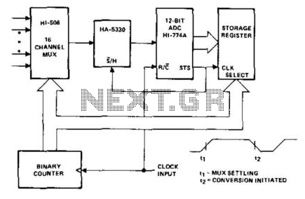
The HI-506 multiplexer functions as an analog input selector, which is controlled by a binary counter to select the appropriate channel. The HA-5330 serves as a high-speed sample and hold circuit. The sample/hold control is connected to the status...
Datagoo is based on the ATMEGA328P microcontroller, widely used by hobbyists in various Arduino projects. It can be programmed via any computer with a USB port when paired with an FTDI FT232RL USB-Serial circuit. Cost-effectiveness and simplicity were prioritized...
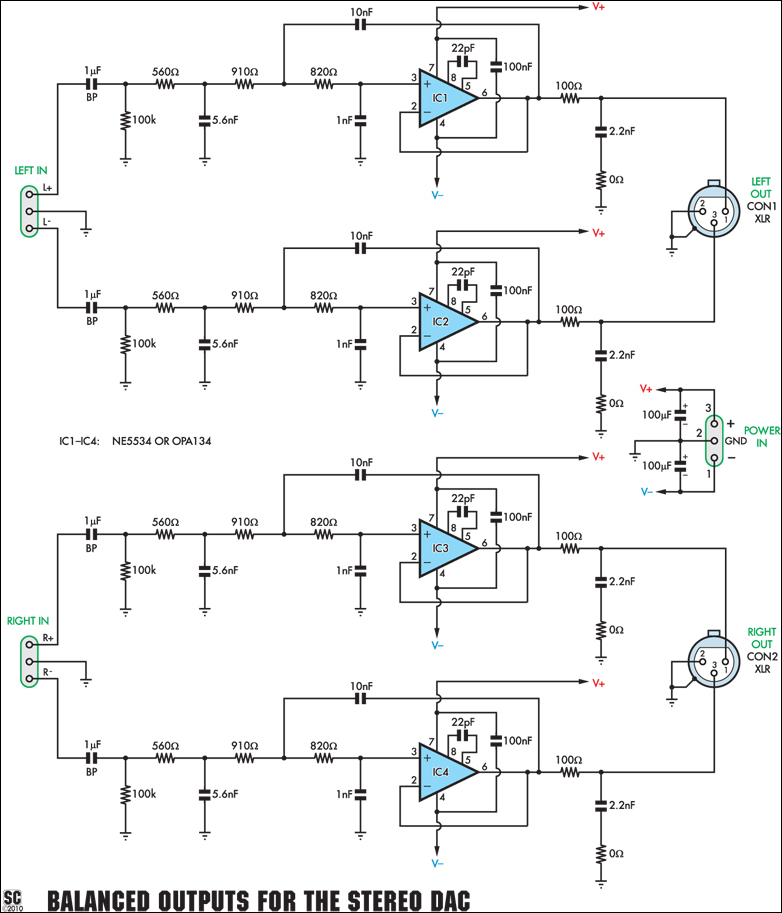
This add-on board is designed to provide a pair of balanced audio outputs for the High-Quality Stereo DAC (Digital to Analog Converter). Two 3-pin male XLR connectors are used for the new outputs, which can either replace or augment...

The SA9618A is designed for ALPC and signal conversion between a CD optical pickup and a decoding chip. This integrated circuit (IC) features an interconnection for a general CD optical pickup photodiode bias voltage VREF generation circuit, an RF...