
Analog to Digital Conversion
Normal operation begins with a high-to-low transition of the WR input, which resets the internal SAR latches and shift-register stages, setting the INTR output high. As long as the CS and WR inputs remain low, the A/D converter stays in a reset state. Conversion starts one to eight clock periods after at least one of these inputs transitions from low to high. After the necessary clock pulses complete the conversion, the INTR pin transitions from high to low, which can be used to interrupt a processor or signal the availability of a new conversion. A read operation (with CS low) will reset the INTR line high again. The device can operate in free-running mode by connecting INTR to the WR input with CS equal to 0. As an 8-bit A/D converter, it represents a voltage range from 0 to 5V, where 0V is represented as 0000 0000 (0 in decimal) and 5V as 1111 1111 (255 in decimal). To convert a value X volts to decimal, a specific formula is used. For improved resolution and to display the value as a floating-point number, the numerator can be multiplied by a factor of 100, 1000, etc., before printing the voltage.
The provided code snippet includes the necessary initialization and operational logic for interfacing with the ADC0804LCN. It defines the input/output pins for reading, writing, and the interrupt signal. The main function initializes the I/O and enters a continuous loop where it waits for the INTR signal to indicate the completion of an A/D conversion. Once the conversion is complete, the code reads the digital voltage value from the designated port and can subsequently display it in decimal form.
The schematic for this application will include the ADC0804LCN connected to an analog signal source, with the reference voltage set appropriately. The microcontroller or processor will be connected to the ADC's control pins (WR, RD, CS, and INTR) and the data output pins will connect to the LCD display for voltage readout. Proper decoupling capacitors should be placed near the power supply pins of the ADC to ensure stable operation. Additionally, the analog input should be conditioned to fit within the 0-5V range to avoid damage to the A/D converter and ensure accurate readings.To be able to implement analog to digital conversion using the ADC0804LCN 8-bit A/D converter. You will design a circuit and program the chip so that when an analog signal is given as input, the equivalent digital voltage is displayed on an LCD display. Thus, in effect, your circuit should function like a simple voltmeter. The ability to convert a nalog signals to digital and vice-versa is very important in signal processing. The objective of an A/D converter is to determine the output digital word corresponding to an analog input signal. The Datasheet for ADC0804LCN shows the pinout and a typical application schematic. The A/D converter operates on the successive approximation principle. Analog switches are closed sequentially by successive-approximation logic until the analog differential input volatge[Vin(+) - Vin(-)] matches a voltage derived from a tapped resistor string across the reference voltage.
The normal operation proceeds as follows. On the high-to-low transition of the WR input, the internal SAR latches and the shift-register stages are reset, and the INTR output will be set high. As long as the CS input and WR input remain low, the A/D will remain in a reset state. Conversion will start from 1 to 8 clock periods after at least one of these inputs makes a low-to-high transition.
After the requisite number of clock pulses to complete the conversion, the INTR pin will make a high-to-low transition. This can be used to interrupt a processor, or otherwise signal the availability of a new conversion. A RD operation(with CS low) will clear the INTR line high again. The device may be operated in the free-running mode by connecting INTR to the WR input with CS=0. Since this is an 8-bit A/D converter, a voltage from 0-5V. O will be repersented as 0000 0000 (0 in decimal) and 5V is represented as 1111 1111 (256 in decimal).
To convert a value X volts to decimal, use the following formula: To get a better resolution, and display the vlaue as a floating point number, you can multiply the numerator by a factor of 100, 1000 etc. and then print the voltage accordingly. #include
🔗 External reference
Related Circuits
Analog-to-digital converters (ADCs), printed-circuit board (PCB), microcontroller or digital signal processor (DSP), total-harmonic-distortion (THD), signal-to-noise ratio (SNR). Analog-to-digital converters (ADCs) are essential components in modern electronic systems, enabling the conversion of analog signals into digital form for processing by microcontrollers...

This digital volume control has no pot to wear out and introduces almost no noise in the circuit. Instead, the volume is controlled by pressing UP and DOWN buttons. This simple circuit would be a great touch to any...
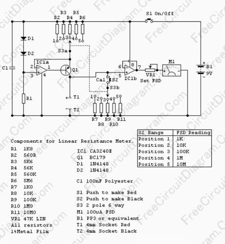
Many analog ohm meters have a non-linear scale, which results in poorer resolution at higher resistance values. This is due to the use of inexpensive current sources. Many analog ohm meters operate on a principle where the scale is not...
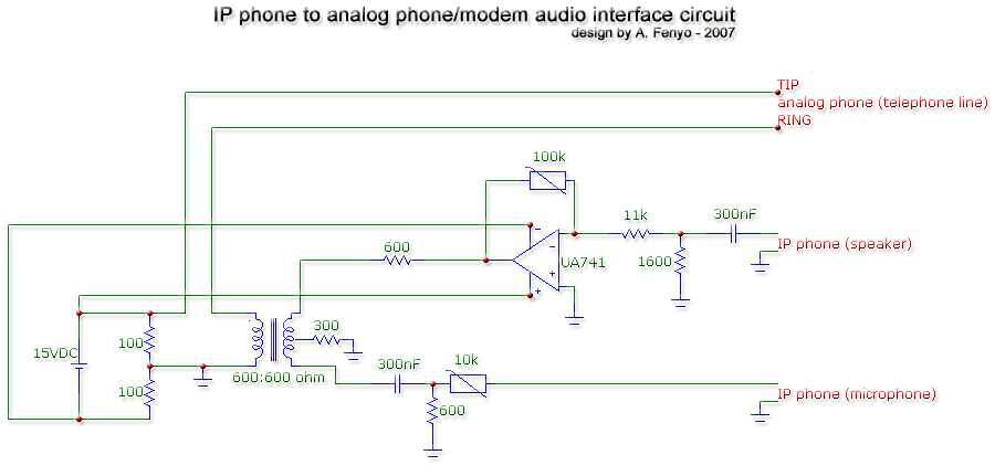
The transformer is a 600:600 ohm transformer, also referred to as a 1:1 ratio 600 ohm transformer. It has approximately the same number of turns on both the primary and secondary coils and is optimized for operation at a...
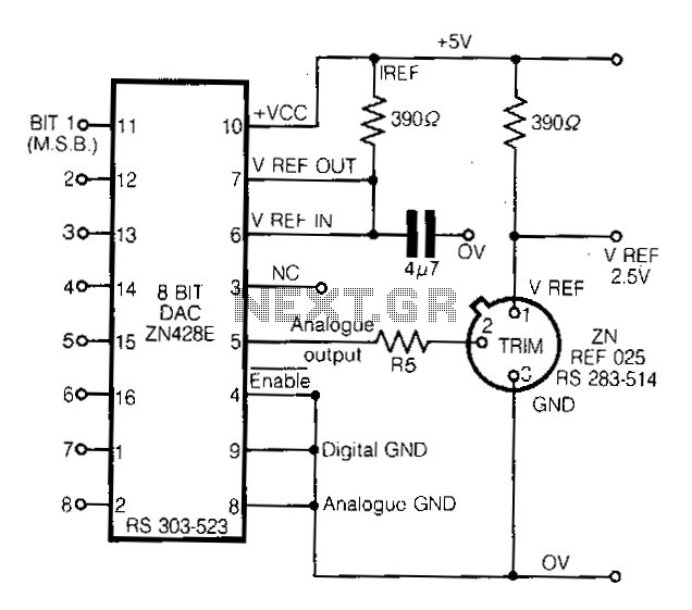
This circuit demonstrates a straightforward approach to achieving a voltage reference that can be adjusted using an 8-bit Digital-to-Analog Converter (DAC) equipped with an integrated voltage reference. The analog output from the DAC controls the trim pin of the...
The C620 lathe Y-conversion includes a power-saving circuit designed for controlling the motor's reversing functionality. This system is applicable to machines such as the C620, C630, and CW61100A lathes, as well as radial drilling and milling machines. The C620 lathe...