
Boost has a frequency characteristic of automatic offset MAX630 power conversion

The described circuit employs the MAX630 integrated circuit, which is specifically designed for low battery detection and boost conversion applications. In this configuration, the resistors R3 and R4 form a voltage divider that continuously monitors the battery voltage. The output from this divider is fed to pin 1 of the MAX630. When the battery voltage falls below the predetermined threshold, the LBD output signal transitions to a low state, indicating a low battery condition.
Upon detection of this low voltage condition, the internal circuitry of the MAX630 responds by connecting capacitors C1 and Cx. This connection is critical as it alters the operational frequency of the internal oscillator. By reducing the oscillator frequency, the circuit compensates for the reduced battery voltage by increasing the output power, thus ensuring that the output voltage remains stable at 5V despite the decline in input voltage.
The overall design emphasizes efficiency and reliability in low voltage conditions, making it suitable for battery-operated devices where maintaining a consistent output voltage is essential. The use of the MAX630 allows for effective power management, ensuring that devices can operate reliably even as their power source depletes. This circuit is particularly beneficial in applications where battery longevity is crucial, as it adapts to changing voltage levels to sustain performance. As shown is a low voltage frequency use MAX630 low battery voltage detection function constitutes offset boost converter power supply. It features when the battery voltage is b elow the nominal value (3V) a lot of time (down to 2V), still at the output high efficiency (85%) to provide a DC voltage 40mA, 5V of. The process is the decline in battery voltage, causing MAX630 1 pin voltage (by R3 and R4 for dividing the battery voltage obtained) also dropped, the current drops below the battery voltage detection comparator threshold voltage (1.31V), the detection output end ( feet) LBD goes low (ground), the C1 and Cx and connected together, thereby reducing the MAX630 internal oscillator frequency.
Increase the output power to compensate for the decrease in the output voltage of the battery power shortage, keeping the output power constant.
Related Circuits
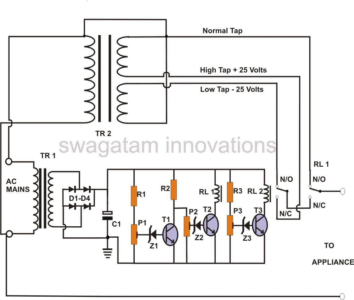
This power stabilizer circuit utilizes one relay to select either the high or low tap from the stabilizer transformer at a specific voltage level. The second relay maintains the normal mains voltage, but when a voltage fluctuation occurs, it...
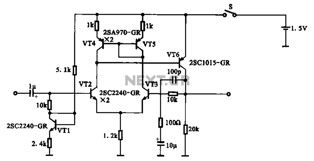
A 1.5V-powered microphone signal amplifying circuit is designed with a power supply for the microphone signal amplification. The circuit primarily consists of a differential amplifier formed by transistors VT2 and VT3. Additionally, VT6 functions as a common emitter voltage...
The CAMD CM8870 CM8870C offers complete DTMF receiver functionality by combining both the band-split filter and digital decoder capabilities into a single 18-pin DIP, SOIC, or 20-pin PLCC package. The CM8870C is produced using advanced CMOS process technology, ensuring...
The schematic circuit design is for a 250-watt output inverter. To increase the power of the circuit, additional Q7 and Q8 transistors can be added in parallel; each pair contributes an additional 250 watts. For instance, to achieve 750...

A hoist rated at 22kW and below is equipped with a power-saving Y-conversion circuit, as depicted in the figure. This circuit enhances the standard hoist design by incorporating a CJ20-10A exchange contactor. The implementation of the Y-conversion circuit during...
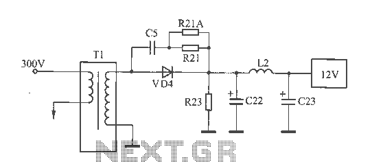
The 12V voltage instability should first be investigated by checking the output section of the switching power supply, as illustrated in the accompanying figure. The secondary winding of the transformer and the switch VD4 have been examined and found...