
Car Battery Charger Circuit

The described circuit operates as a current-limited battery charger, specifically designed for charging a 6V car battery. The primary function of the circuit is to ensure that the charging current does not exceed 4.2A, which is crucial for maintaining battery health and preventing damage from overcharging.
The operation begins with the sensing resistor R1, which has a voltage drop of 600mV when a current of 4A flows through it. This voltage drop triggers the conduction of transistor T1, which plays a critical role in regulating the charging process. By controlling the base current of T3, T1 ensures that the charging current remains within the safe limit, thereby preventing excessive charging that could lead to battery degradation.
Transistor T4, a 2N3055, functions as the main power transistor in this circuit. It is responsible for delivering the required load current to the battery while maintaining the voltage difference between the battery and the load. The collector-emitter junction of T4 is where the load current is balanced against the actual battery voltage, ensuring efficient charging.
The power dissipation in T4 is a key consideration, especially when charging a 6V battery at a maximum power of 40W. This is calculated as the product of the load current and the voltage difference across T4. To manage the heat generated during operation, it is essential to mount the 2N3055 on a robust heatsink, which will allow for adequate thermal management and prevent thermal runaway conditions.
In addition, the rectifier diodes used in the circuit must be rated to handle at least 4A at 40V to ensure reliable operation during the charging process. The choice of diodes should also consider factors such as reverse recovery time and forward voltage drop to optimize overall efficiency.
Overall, this circuit design exemplifies effective battery management through current limiting, thermal protection, and efficient power delivery, making it suitable for automotive applications where reliable charging is essential.The car battery charging current is automatically limited to 4. 2A. If there is a 600mV voltage on R1 (4A thru it), then the T1 transistor starts to conduct. Excessive charging current is avoided because the current value on T3 ²s base is limited. The difference between applied load current (at T4 ²s collector) and real voltage of the battery is balanced thru T4 ²s collector-emitter junction. The power input of T4 (2N3055) is the product of load current and voltage difference already mentioned. When charging 6V car battery this power reaches a maximum of 40W. The rectifier diodes must be able to deliver 4A at 40V. T4 2N3055 must be mounted on a good heatsink in order to dissipate the heat. 🔗 External reference
Related Circuits
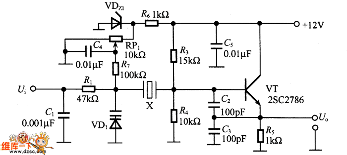
The figure illustrates the FM modulation circuit of a crystal oscillator. FM modulation can be achieved through direct and indirect methods. The direct FM method involves directly altering the frequency of the oscillating circuit. While this approach is straightforward,...
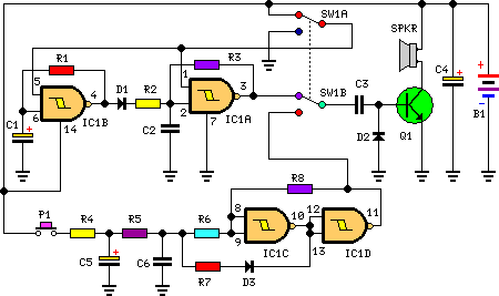
This circuit is designed for children's entertainment and can be installed on bicycles, battery-powered cars, motorcycles, as well as models and various games and toys. When switch SW1 is positioned as indicated in the circuit diagram, it generates the...
Examples of an OFDM modulation system. The graph illustrates the input data signal (.... --- Ol01100) and the data signal by the string. The input signal is separated into components such as "00", "ll", "10", "00", "01", and other...
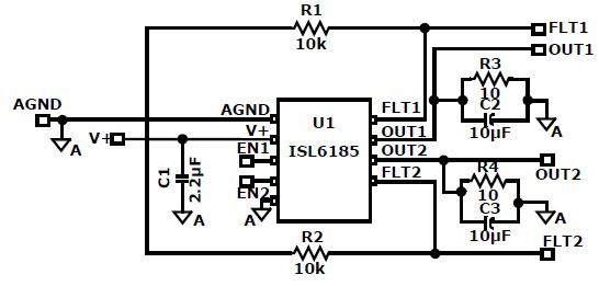
The ISL6185 USB power controller family can be utilized to design a straightforward USB power supply electronic project that offers fully independent overcurrent (OC) fault protection for two or more USB ports. This product family includes sixteen distinct functional...
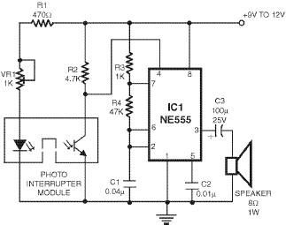
This smoke detector utilizes a 555 timer circuit along with common electronic components. The photo interrupter module serves as the smoke detection element, while the 555 timer is configured in astable mode to function as an audio frequency oscillator,...
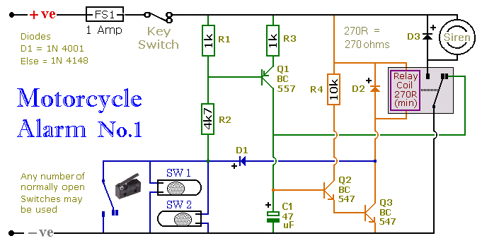
This circuit includes a timed output and an automatic reset feature. It can be manually operated using a key switch or a concealed switch. By incorporating an external relay, the circuit will automatically engage or immobilize the machine each...