
Audio Amplifiers 8
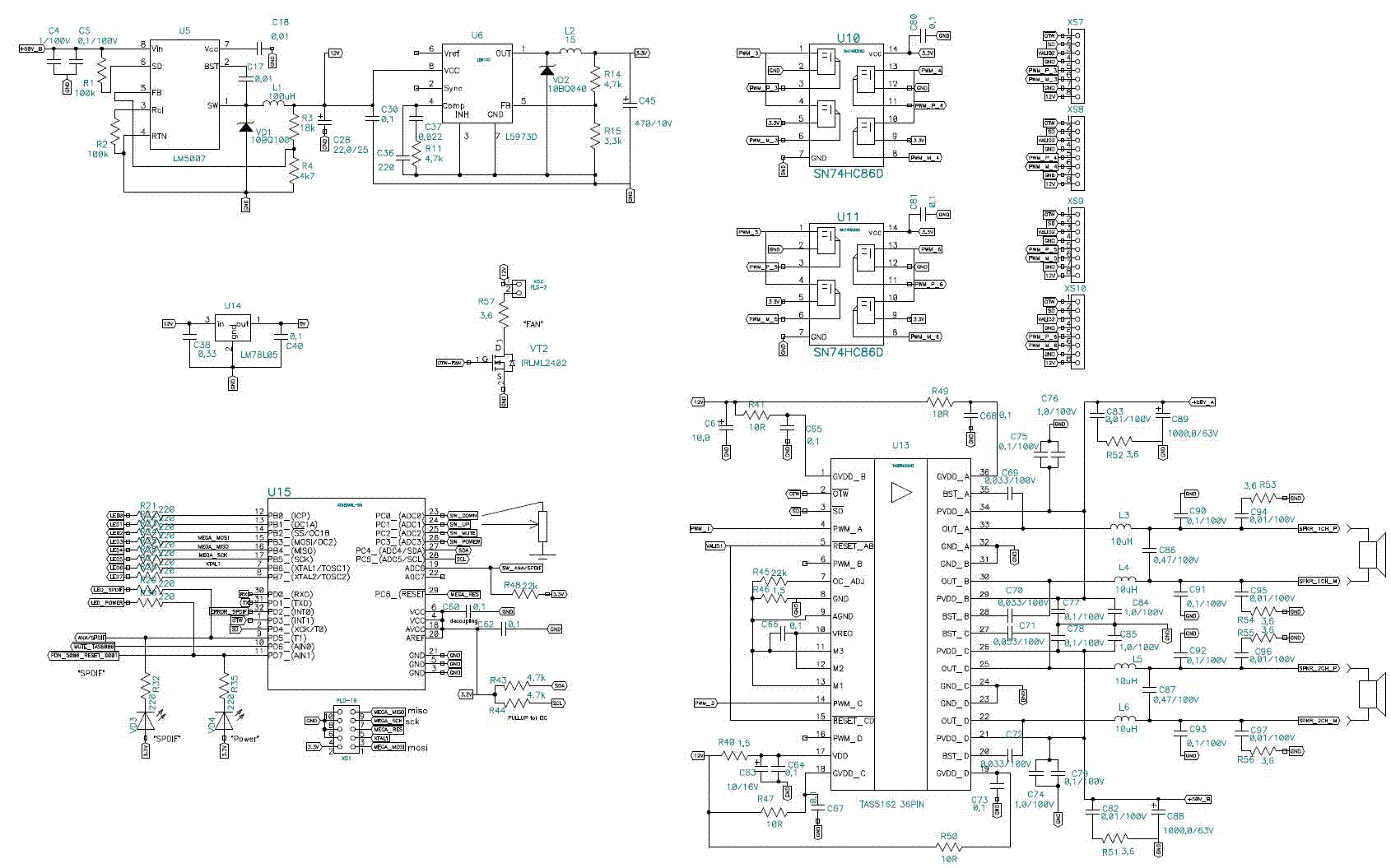
The Class-D amplifier design incorporates the TAS5162, PCM1808, and TAS5086, which are critical components for achieving high efficiency and sound quality. The TAS5162 serves as the main amplifier, while the PCM1808 functions as the analog-to-digital converter (ADC) for input signal processing. The TAS5086 is used for digital signal processing and managing power states, including entering protection modes under fault conditions.
The issues reported by users highlight potential thermal management challenges and the importance of proper circuit design to prevent overheating of the TAS5162. The protection mode activation indicates that the amplifier is designed to safeguard itself against excessive current or thermal stress. The design must ensure adequate heat dissipation, possibly through heat sinks or PCB thermal management techniques.
The modulation of the output signal when the supply voltage exceeds specified limits suggests that the amplifier's output stage may be experiencing clipping or distortion, which can lead to undesirable audio performance. The implementation of a well-designed low-pass filter is critical for maintaining signal integrity and preventing high-frequency noise from affecting the audio output.
Further investigation into the grounding scheme is warranted, as excessive parasitic inductance can adversely affect the performance of the amplifier. Grounding should be optimized to minimize inductance and ensure stable operation. Additionally, the placement of decoupling capacitors is vital to maintain voltage stability at the power pins, which can significantly influence the performance and reliability of the amplifier.
The selection of inductors for the output stage must consider the current handling capabilities and inductance values to avoid saturation under load conditions. Following the guidelines for output filter design and ensuring proper loading conditions during testing will contribute to the overall stability and performance of the Class-D amplifier.a year ago I designed a class-D amplifier based on the TAS5162, pcm1808 and TAS5086. During the year, was made a few hundred samples intended to be sold to radio amateurs. Most devices are functioning properly and not cause any complaints from consumers. But some instances do not work properly. in some cases, users complain about the failure of these chips in the long run the amplifier (more than 30min). First TAS5162 overheats and goes into protection mode, and then closes the power PVDD to GND, GND_x. Then comes the smoke and body chip breaks. 4. Why increase the supply voltage over 37V (Rl = 4Ohm - resistor) causes modulation of the output signal from the noise This triggered a primary protection OCP Sometimes there is a click when connecting / disconnecting the input from pcm1808. Then the sound just disappears. No reset or hardware enable / disable (pins PDN, RST) TAS5086 does not return it to normal operation.
Only after the power cycling circuit begins to operate normally. The same problem sometimes happens in my other amplifier on the basis of TAS5504 b) WhenSD isset low by TAS5162, microcontroller U15 sets TAS5086 to PDN mode. If SD returns to normal state (high), U15 restarts TAS5086 to operating conditions. 6. Last week I tried to course abnormal functioning of the device, then TAS5162 goes to protection state or fails.
Following your post «The low pass filter is critical to the operation of the chip » I used CDRH127/LD-100NC in channel no. 1, and self-made coil inductors in channel no. 2, so I could observe their influence. During the increase of input signal level, the sine signal on the exit begins to be limited by supply voltage and gets a square form.
BUT! At the certain moment it`s modulated with about 50kHz sine. It looks like autogeneration As we can see in the picture, the output voltage accepts also the subzero values up to -20V. I understand, that CDRH127 is not powerful enough for TAS5162 with load impedance 4Ohm (PVDD<=38, 5). But how does the inductor influence, if in tested circuit we have no load impedance I read SLYT198 TI document (see attach.
). There is posted, that The designer who is primarily concerned with maximum heat and power-supply constraints and is not concerned with EMI and cuiescent current could use the Class-D amplifier without a filter to save cost . But actually it appears that the amplifier is very choosy to filter presence, and even more to its quality.
Thank you for sharing your Gerber files. I am concerned that the grounding for the TAS5162 may contain too much parasitic inductance between the input ground and the output grounds. Also, the decoupling capacitors for the PVDD pins should be placed no more than 2mm from their pins and 1mm is preferred.
If you update your PCB, please refer to the TAS5162DKD6EVM User`s Guide (SLAU223) for PCB layout suggestions. I would not advise routing PCB traces under the device, particularly in the top layer. I am working on getting a recommendation for an output inductor vendor;however, a good "rule of thumb" is that the inductor should deliver at least 5uH of inductance at twice the overcurrent limit of the device.
The starting value is 10uH and its value can sag due to saturation and temperature effects. In your case, with a 22K over current resistor, your over current limit should be ~12 Amps, so your inductor should be capable of at least 5uH of inductance at 24 Amps. The paper you cited on output filters does not apply to a high power Class D power stage like this one.
Class D amplifiers with LC output filters should not be tested without a load. Without a load, the filter will begin to oscillate and cause an over voltage condition. I understand that your oscilloscope traces were taken at the output of the filter; however, you will probably find similar waveforms at the output pins of the TAS5162. The Absolute Maximum Voltage for this device is -0. 3V to 71V and in your te 🔗 External reference
Related Circuits
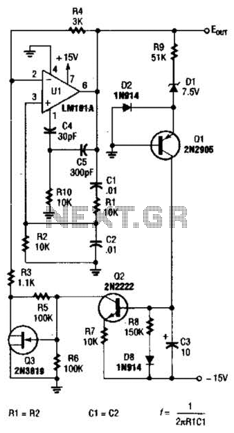
For variable-frequency operation, Rl and R2 can be replaced by a dual potentiometer. In electronic circuits that require variable-frequency operation, the use of a dual potentiometer as a replacement for resistors Rl and R2 can provide enhanced functionality and flexibility....
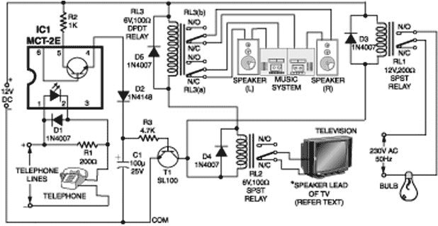
A telephone line-based audio muting and light activation circuit. Frequently, when listening to music or watching television at elevated volume levels, it becomes difficult to hear a telephone ring, resulting in missed important calls. This circuit is designed to address...
This circuit is designed to connect stereo outputs from four different sources or channels as inputs, allowing only one of them to be selected and connected to the output at any given time. When the power supply is turned...
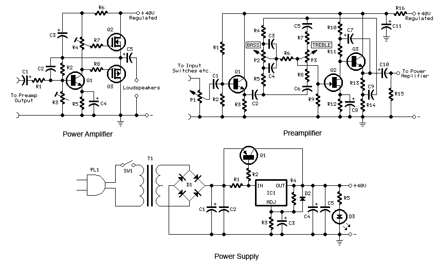
Parts List The circuit consists of a preamplifier, tone controls, and a regulated DC power supply, providing a power output of 18 Watts for an 8 Ohm load. The circuit design includes three main components: a preamplifier, tone control circuitry,...
An audio mixer receives outputs from various audio sources and amplifies them to drive a common speaker, allowing all active radios to be heard through a single speaker. However, there is a need for a master Audio On/Off switch...
This design circuit functions to filter out interference signals, ensuring that the signal received from a Morse code station is distinct. The circuit utilizes the earliest mode of radio communications, which employs Morse Code on a continuous wave carrier...