
IRF9540N Gate Charge Test Circuit Schematic and Datasheet

The IRF9540N Gate Charge Test Circuit is designed to evaluate the gate charge characteristics of the IRF9540N MOSFET. This circuit typically consists of a power supply, a resistor to limit the gate current, and measurement equipment to capture the gate charge waveforms. The gate charge, denoted as Qg, is critical for understanding the switching performance of the MOSFET, as it influences the turn-on and turn-off times.
The circuit operates by applying a voltage to the gate of the IRF9540N while monitoring the current through the gate resistor. The charge accumulated on the gate capacitance can be determined by integrating the gate current over time. The results provide insights into the efficiency of the MOSFET in various applications, particularly in high-frequency switching scenarios.
Furthermore, the datasheet's inclusion of the Switching Time Test Circuit and associated waveforms allows for a comprehensive analysis of the IRF9540N's performance in dynamic conditions. The Unclamped Inductive Test Circuit evaluates the device's response to inductive loads, while the Peak Diode Recovery dv/dt Test Circuit assesses the recovery characteristics of the body diode under high dv/dt conditions. Collectively, these tests provide a thorough understanding of the IRF9540N's operational limits and suitability for specific applications in power electronics.IRF9540N Gate Charge Test Circuitis schemed in the diagram below. IRF9540N is known to be rectifier device with advanced processing techniques to achieve extremely low on resistance per silicon area, according to the datasheet. Other thanGate Charge Test Circuit Schematic, you will find such Switching Time Test Circuit and Waveforms, Unclamped Ind
uctive Test Circuit, and Peak Diode Recovery dv/dt Test Circuit in the depth of the IRF9540 datasheet. 🔗 External reference
Related Circuits
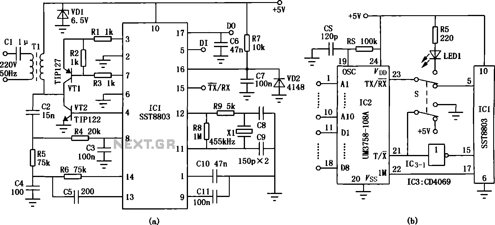
The transmission circuit for inductive wireless headsets must be securely mounted on a wall or ceiling, limiting its outdoor usability, which is a significant disadvantage of inductive wireless headphones. In contrast, infrared wireless headsets utilize a compact infrared transmitter...
Logic-1 and logic-0 represent the states of digital signals, where logic-1 corresponds to a high voltage close to Vcc, and logic-0 corresponds to a voltage near neutral or ground. Logic-0 cannot be transformed into logic-1, while logic-1 can revert...
This circuit is designed to charge NiCad battery packs within the voltage range of 4.8 to 15.6 V using a convenient remote power source, such as an automobile battery. Upon initial power application, a small bias current supplied by...
TCRT1000 - Reflective Optical Sensor manufactured by Vishay Semiconductors. This component was ordered from Mouser. For more information, refer to the Sensor Report on the Reflective Optical Sensor TCRT1000. While there are concerns regarding the code and schematic used,...
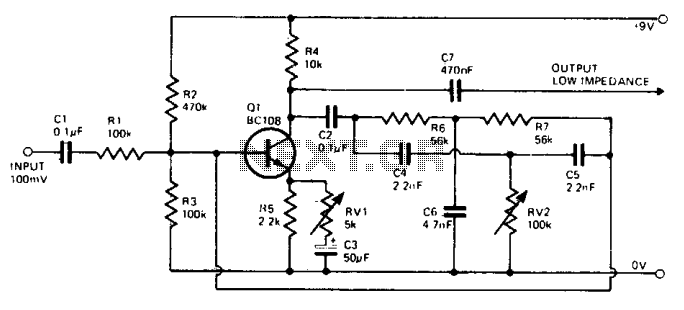
The wah-wah effect is created when specific frequencies are amplified more than others. The fundamental circuit consists of a phase shift RC oscillator. Negative feedback is implemented by returning a portion of the signal to the base. During initial...
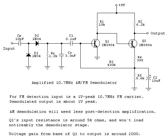
Frequency-to-voltage converters are integral components in various instrumentation circuits and are also utilized in radio applications as FM demodulators. A notable configuration for these applications is the Diode Charge Pump circuit (DCP), which additionally serves as an AM detector....