


Square wave generator with CD4070
#CD4070
#square wave
#CMOS
#2 MHz
#signal generator
#digital oscillator
#waveform generation
#frequency generator
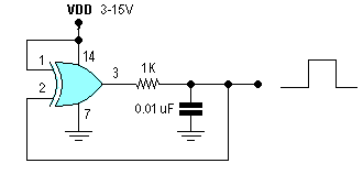
Description: Square wave generator using the CD4070. This circuit can generate square waves up to 2 MHz. The CD4070 CMOS is utilized in this example.
The square wave generator circuit based on the CD4070 integrated circuit (IC) is an effective solution for producing high-frequency square wave signals, capable of reaching frequencies up to 2 MHz. The CD4070 is a quad 2-input XOR gate CMOS device, which can be configured to create oscillations by utilizing feedback and external components.
In this configuration, two XOR gates from the CD4070 are employed. The first XOR gate receives a clock signal, which is typically generated by a resistor-capacitor (RC) timing network. The timing components, such as a resistor (R) and a capacitor (C), determine the frequency of the oscillation. The output of the first XOR gate is fed back into the second XOR gate, which further shapes the waveform.
The power supply voltage (VDD) for the CD4070 should be carefully chosen; it typically ranges from 3V to 15V, depending on the desired output characteristics. Proper bypass capacitors should be placed near the power supply pins of the IC to filter out noise and ensure stable operation.
The output of the circuit can be connected to various loads, such as LEDs for visual indication or further processing stages in digital circuits. The square wave signal generated can be used in applications such as clock generation for digital circuits, waveform generation for testing, and as a timing reference in various electronic systems.
To ensure optimal performance, it is essential to consider the characteristics of the components used, including the tolerance of resistors and capacitors, as these will affect the frequency stability and the duty cycle of the output waveform. Additionally, the layout of the circuit should minimize parasitic capacitance and inductance to maintain signal integrity at high frequencies.Square wave generator with CD4070. with this circuit it can generate square wave up to 2 MHz In this example I use CD4070 CMOS. VDD :.
The square wave generator circuit based on the CD4070 integrated circuit (IC) is an effective solution for producing high-frequency square wave signals, capable of reaching frequencies up to 2 MHz. The CD4070 is a quad 2-input XOR gate CMOS device, which can be configured to create oscillations by utilizing feedback and external components.
In this configuration, two XOR gates from the CD4070 are employed. The first XOR gate receives a clock signal, which is typically generated by a resistor-capacitor (RC) timing network. The timing components, such as a resistor (R) and a capacitor (C), determine the frequency of the oscillation. The output of the first XOR gate is fed back into the second XOR gate, which further shapes the waveform.
The power supply voltage (VDD) for the CD4070 should be carefully chosen; it typically ranges from 3V to 15V, depending on the desired output characteristics. Proper bypass capacitors should be placed near the power supply pins of the IC to filter out noise and ensure stable operation.
The output of the circuit can be connected to various loads, such as LEDs for visual indication or further processing stages in digital circuits. The square wave signal generated can be used in applications such as clock generation for digital circuits, waveform generation for testing, and as a timing reference in various electronic systems.
To ensure optimal performance, it is essential to consider the characteristics of the components used, including the tolerance of resistors and capacitors, as these will affect the frequency stability and the duty cycle of the output waveform. Additionally, the layout of the circuit should minimize parasitic capacitance and inductance to maintain signal integrity at high frequencies.Square wave generator with CD4070. with this circuit it can generate square wave up to 2 MHz In this example I use CD4070 CMOS.
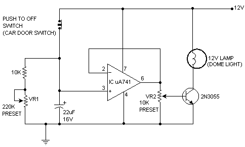
Bistable Multivibrators
The circuit utilizes a CMOS dual D flip-flop (CD4013) to toggle a relay or other load using a momentary push button. Multiple push buttons can be connected in parallel to control the relay from different locations. A high signal from...
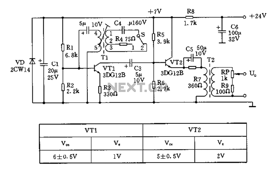
450 800Hz signal generator circuit diagram
The 450/800Hz oscillation circuit depicted in the figure utilizes transformer coupling. The frequency conversion is achieved by varying the inductance through a variable filter tap (T1). When the switch control signal (S) is set to position 1, the oscillator circuit...
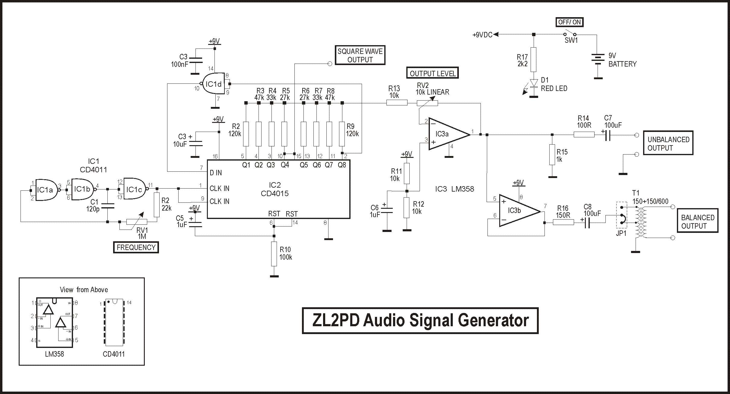
Audio Signal Generator
A couple of inexpensive CMOS integrated circuits are utilized to digitally generate audio sine waves across a broad frequency range in this compact battery-operated test instrument. The oscillator features both unbalanced and balanced outputs. Signal generators are frequently used in...
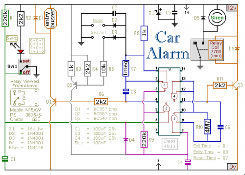
cmos based vehicle anti theft alarm
This car alarm circuit includes Exit and Entry delays, an instant alarm zone, an intermittent siren output, and an automatic reset function. By incorporating external relays, it is possible to immobilize the vehicle and activate the lights.
The car alarm circuit...
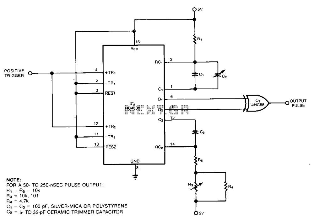
Cmos-short-pulse-generator
The pulse generator consists of two low-power CMOS chips that produce a precise pulse width ranging from 50 to 500 ns. IC1 is a dual monostable multivibrator (one shot) where each positive trigger pulse initiates simultaneous positive output pulses at...
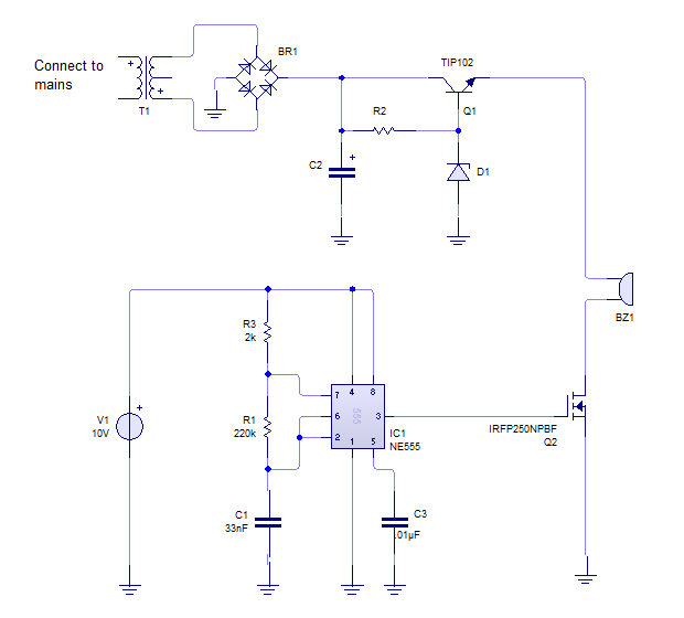
How to amplify a square wave cheaply
A piezo disk is being driven at a frequency of 100 Hz or lower, with the output from the signal generator limited to 10 V. The goal is to amplify this output to 50 or even 100 Volts.
To achieve the...
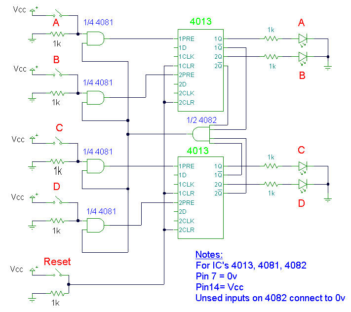
Quiz Circuit
This design utilizes four integrated circuits (ICs) and features four input circuits with four independent outputs, along with a single master reset switch. The outputs are configured with light-emitting diodes (LEDs), which can be modified to control lamps or buzzers....
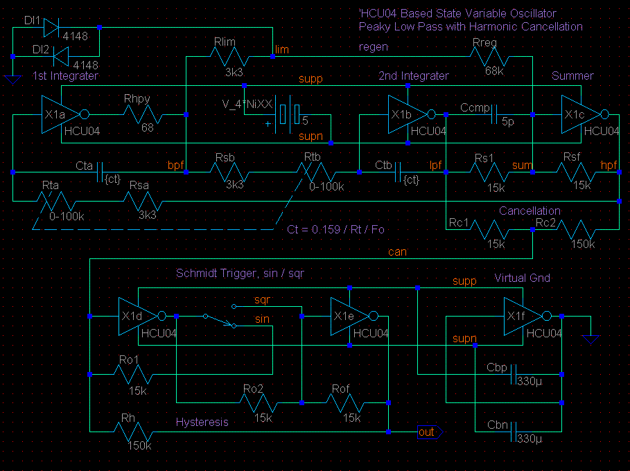
CMOS Un-Buffered Inverter based Sine / Square Generator
This circuit is based on the State Variable Band Pass Filter, incorporating amplitude-limited regenerative feedback.
The State Variable Band Pass Filter (SVBPF) is a versatile filter design that allows for simultaneous control over the center frequency, bandwidth, and gain. This filter...
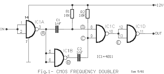
frequency doubler with 4011
This frequency doubler utilizes a CMOS quad two-input NAND gate package, specifically the 4011 type. The core of the frequency doubler includes an inverter (IC1B) along with two differentiating networks composed of resistors (R1, R2) and capacitors (C1, C2). The...