
synthesized PLL for Low Power FM transmitter
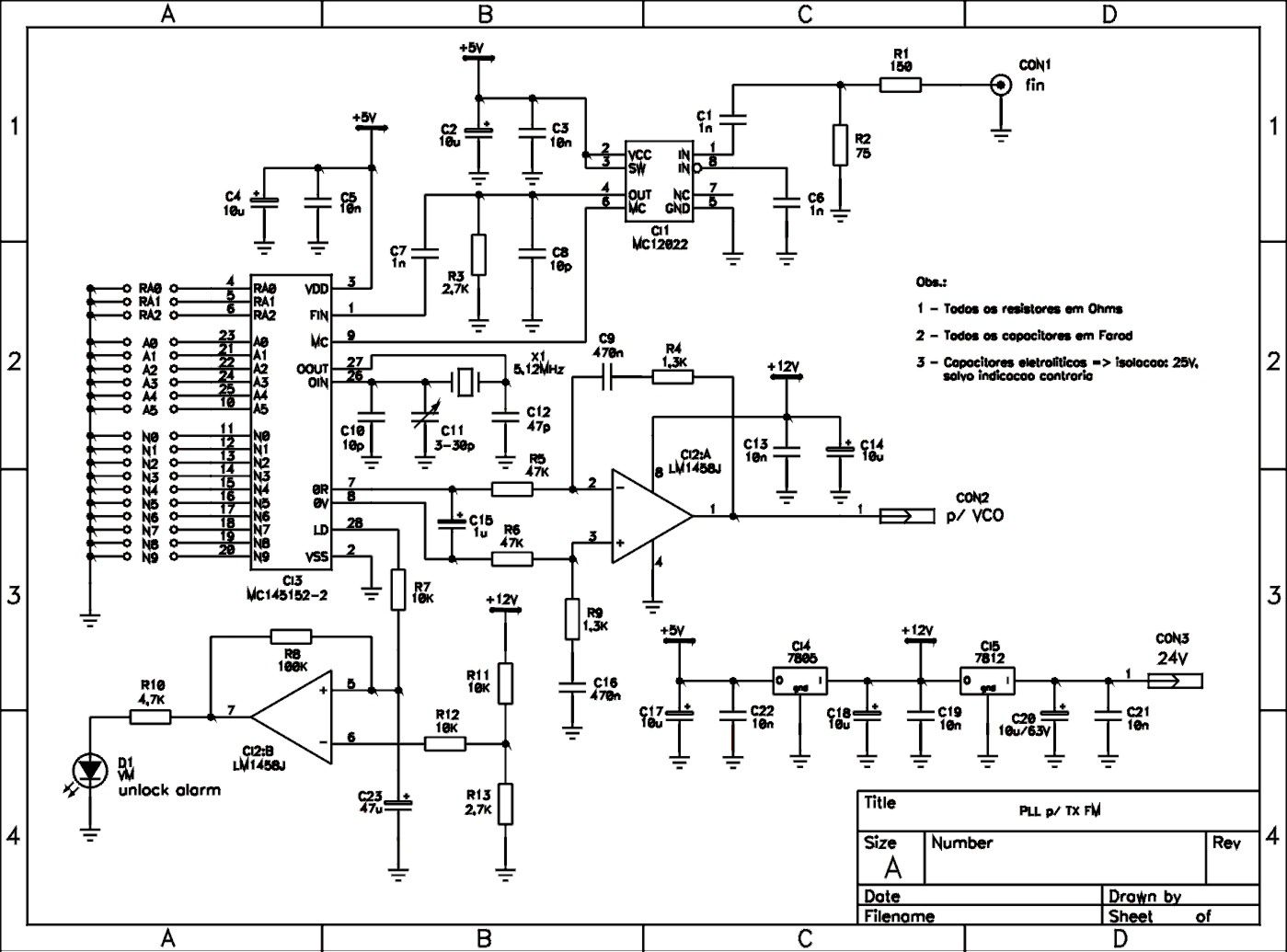
The synthesized PLL circuit is a critical component in low-power FM transmitter designs, allowing for precise frequency control and stability. The architecture generally consists of a voltage-controlled oscillator (VCO), a phase/frequency comparator, and a loop filter. The VCO generates an output frequency that can be adjusted based on the input control voltage. The phase/frequency comparator compares the output frequency of the VCO with a reference frequency derived from the crystal oscillator. The output of the comparator is used to adjust the control voltage applied to the VCO, ensuring that the VCO frequency locks onto the desired frequency.
In this design, the use of a 5.12 MHz crystal reference is essential for achieving the required frequency steps. The selection of the R divider value (R=512) is crucial, as it determines how the reference frequency is scaled down to match the VCO frequency. This allows for finer frequency adjustments and ensures compatibility with the FM channel spacing requirements.
The prescaler (P=40) reduces the input frequency to a manageable level for the PLL, allowing it to function correctly within its specified input frequency range. The downconversion process is necessary because the phase/frequency comparator has a limited operating frequency range. By ensuring that the input frequency does not exceed 10 MHz or 15 MHz, the PLL can maintain accurate phase and frequency comparisons, leading to stable operation.
The flexibility of this PLL design enables it to be adapted for use in various applications beyond low-power FM transmission. By recalibrating the loop filter and VCO components, as well as adjusting the programming keys and crystal values, this circuit can be tailored to meet specific frequency stability and locking requirements for different systems.This is schematic of a synthesized PLL for the Low Power FM transmitter. By the way, you also can use it with other circuits, just pay attention to recalculate the loop filter response and components, VCO tank circuit, and the correct thumbswitch programming keys, crystal value. The original project of FM transmitter was made to operate in both co nfiguration ( synthesized or open loop free oscilattor), with synthesized version you can assure very high frequency stability, and also lock digital FM receivers ( 200KHz step in major of countries). A crystal reference of 5. 12 MHz was employed to assure 10 KHz steps ( enough sufficient to FM channeling of 200 KHz), and it also depends of R divider crystal reference, here I used R=512 to the MC145151P2 of Motorola.
P - is the prescaler divider, normally P=40 to MC12016, the PLL needs downconverter the input frequency ( pin1) because the phase/frequency comparator just work at maximum of 10MHz or 15MHz input frequency. 🔗 External reference
Related Circuits
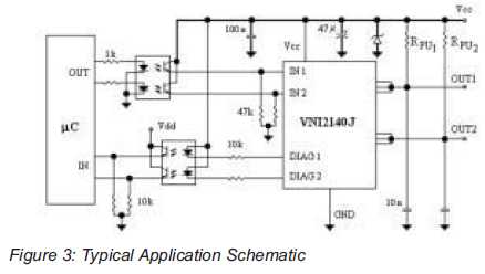
An integrated solution for two output channels that simplifies design and enhances reliability. The device, the VNI2140J, integrates on-chip two 45V Power MOSFET channels with a typical Rds(on) of 80mOhm at 25 degrees Celsius. The VNI2140J is a highly integrated...
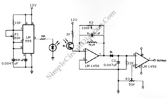
The infrared transmitter and receiver circuit depicted in the schematic diagram below can function as a remote control. The transmitter primarily operates as an oscillator. The infrared transmitter and receiver circuit is designed to facilitate wireless communication through infrared signals,...
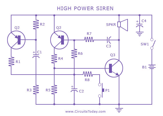
A siren circuit diagram that generates a strong, high-power siren or alarm sound using complementary transistor pairs BC 557 and BC 337, arranged as an oscillator. The described siren circuit employs a pair of complementary transistors, BC 557 (a PNP...
This unique amplifier was designed and built for the European Triode Festival in 2007, focusing on "White Light" amplifiers that utilize thoriated tungsten tubes. Due to the impracticality of transporting a large tube amplifier from the US to Europe,...
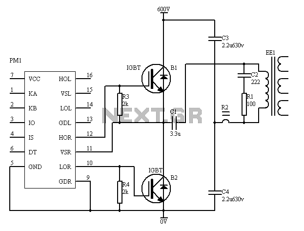
The PM4040F is utilized in switching power supply applications for medium power ranges. It is designed to drive power supplies between 200W and 800W, as illustrated in the accompanying bridge circuit. For power applications below 1000W, an alternative circuit...
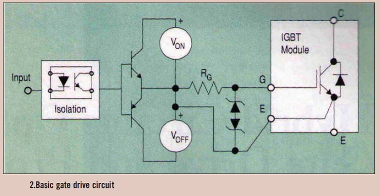
High power IGBT modules utilize hybrid integrated circuit (IC) gate drives that incorporate protection circuits, which implement desaturation detection or real-time control. High power Insulated Gate Bipolar Transistor (IGBT) modules are essential components in various high-efficiency power conversion applications, such...