
Demultiplexer

This circuit reconstructs and separates analog signals that have been time-division multiplexed. The conventional method has several restrictions, particularly when a short dwell time and a long, accurate hold time are required. The capacitors must charge from a low-impedance source through the resistance and current-limiting characteristics of the multiplexer. During the holding phase, the high-impedance lines are relatively long and susceptible to noise pickup and leakage. When FET input buffer amplifiers are utilized for low leakage applications, significant temperature offset errors are often introduced.
This circuit design focuses on the reconstruction and separation of time-division multiplexed analog signals, addressing the limitations of traditional methods. The circuit employs a multiplexer to route signals effectively; however, it faces challenges due to the inherent characteristics of the components involved. The capacitors in the circuit must charge from a low-impedance source, which is critical for maintaining signal integrity. The resistance associated with the multiplexer and its current-limiting features can affect the charging time of these capacitors, particularly when a short dwell time is necessary.
During the holding phase, the circuit operates under high-impedance conditions. This setup is prone to noise interference, which can degrade the quality of the output signals. The length of the high-impedance lines further exacerbates this issue, as longer lines are more likely to pick up electromagnetic interference and experience leakage currents.
To mitigate these problems, the circuit may incorporate FET input buffer amplifiers. These amplifiers are advantageous for their low leakage characteristics, making them suitable for applications where signal preservation is paramount. However, the use of FETs can introduce temperature offset errors, which must be carefully managed to ensure accurate signal reconstruction. Overall, this circuit design exemplifies the complexities involved in handling multiplexed analog signals, emphasizing the need for careful consideration of component selection and circuit layout to achieve optimal performance.This circuit reconstructs and separates analog signals which have been time-division multiplexed. The conventional method, shown on the left, has several restrictions, particularly when a short dwell time and a long, accurate hold time is required. The capacitors must charge from a low-impedance source through the resistance and current-limiting characteristics of the multiplexer.
When holding, the high-impedance lines are relatively long and subject to noise pickup and leakage. When FET input buffer amplifiers are used for low leakage applications, severe temperature offset errors are often introduced.
Related Circuits
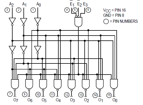
The Motorola SN54/74LS138 is recognized as a 1-of-8 decoder or demultiplexer, specifically engineered for high-speed bar memory chip select address decoding. The accompanying diagram illustrates the logic configuration of the SN54/74LS138 demultiplexer. According to the SN54 datasheet, the multiple...

This circuit functions as a universal decoder, capable of operating either as a dual 1-of-4 decoder or as a single 1-of-8 decoder, depending on the signal applied to the Mode Control (M) input. In the dual mode, each section...