
Dual Power Amplifier Using TDA7293 MOSFET IC

The circuit design focuses on a compact and efficient layout, allowing for the integration of two TDA7293 amplifiers on a single PCB. The choice of MOSFET technology in the TDA7293 allows for better thermal management and lower distortion levels, which are critical for high-fidelity audio applications. The schematic includes all necessary connections for power supply, input, and output, ensuring that the amplifier operates within optimal parameters.
In terms of component selection, the use of high-quality capacitors and resistors is recommended to maintain signal integrity and performance. The layout should prioritize short signal paths and adequate grounding to minimize noise and interference. The inclusion of fusible tracks instead of traditional fuses is a design choice that emphasizes space-saving while still providing a level of fault protection.
The board's compact dimensions make it suitable for various applications, including home audio systems, portable speakers, and other audio equipment where space is at a premium. The ability to operate with a single TDA7293 or dual configurations provides flexibility for users depending on their power requirements. Overall, this project represents a practical solution for those seeking a reliable and space-efficient power amplifier design.As readers will know, there are already several power amplifier projects, two using IC power amps (aka power opamps). Both have been popular, and this project is not designed to replace either of them. However, it is significantly smaller than the others, so it makes building a multiple amp unit somewhat easier because the space demand is much low
er. It`s quite simple to include 4 amps (two boards) into a small space, but be aware that good heatsinking is essential if you expect to run these amps at significant power levels. The TDA7293 IC uses a MOSFET power stage, where the others featured use bipolar transistors. The main benefit of the MOSFET stage is that it doesn`t need such radical protection circuitry as a bipolar stage, so unpleasant protection circuit artefacts are eliminated.
There are no apparent downsides to the TDA7293, although it was found that one batch required a much higher voltage on the Standby and Mute pins than specified, or the amps would not work. This is not a limitation, since both are tied to the positive supply rail and are therefore disabled.
This particular project has been planned for a long time, but for some reason I never got around to completing the board or the project description. This is now rectified, and it`s ready to "rock and roll". The board is very small - only 77 x 31mm, so getting it into tight spaces is easy. provided adequate heatsinking is available of course. The TDA7293 has a bewildering number of options, even allowing you to add a second power stage (in another IC) in parallel with the main one.
This improves power into low impedance loads, but is a rather expensive way to get a relatively small power increase. It also features muting and standby functions, although I`ve elected not to use these. The schematic is shown in Figure 1, and is based on the PCB version. All unnecessary functions have been disabled, so it functions as a perfectly normal power amplifier. While the board is designed to take two TDA7293 ICs, it can naturally be operated with only one, and the PCB is small enough so that this is not an inconvenience.
A LED is included to indicate that power is available, and because of the low current this will typically be a high brightness type. The IC has been shown in the same format that`s shown in the data sheet, but has been cleaned up for publication here.
Since there are two amps on the board, there are two of most of the things shown, other than the power supply bypass caps and LED "Power Good" indicator. These ICs are extremely reliable (as are most power amp ICs), and to reduce the PCB size as much as possible, fuse clips and fuses have not been included.
Instead, there are fusible tracks on the board that will fail if there is a catastrophic fault. While this is not an extremely reliable fuse, the purpose is to prevent power transformer failure, not to protect the amplifiers or PCB. I normally use a gain of 23 (27dB) for all amplifiers, and the TDA7293 is specified for a minimum gain of 26dB, below which it may oscillate.
Although this is only a small margin, tests so far indicate that the amp is completely stable. If you wish, you may increase the gain to 28 (29dB) to give a bit more safety margin. To do this, just change the input and feedback resistors (R3A/B and R4A/B) from 22k to 27k. The circuit is conventional, and is very simple because all additional internal functions are unused. The LED is optional, and if you don`t think you`ll need it, it may be omitted, along with series resistor R3.
All connections can be made with plugs and sockets, or hard wired. In most cases, I expect that hard wiring will be the most common, as the connectors are a pain to wire, and add unnecessary cost as well as reduce reliability. The TDA7293 specifications might lead you to believe that it can use supply voltages of up to ±50V. With zero input signal (and therefore no output) it might, but I don`t reco 🔗 External reference
Related Circuits
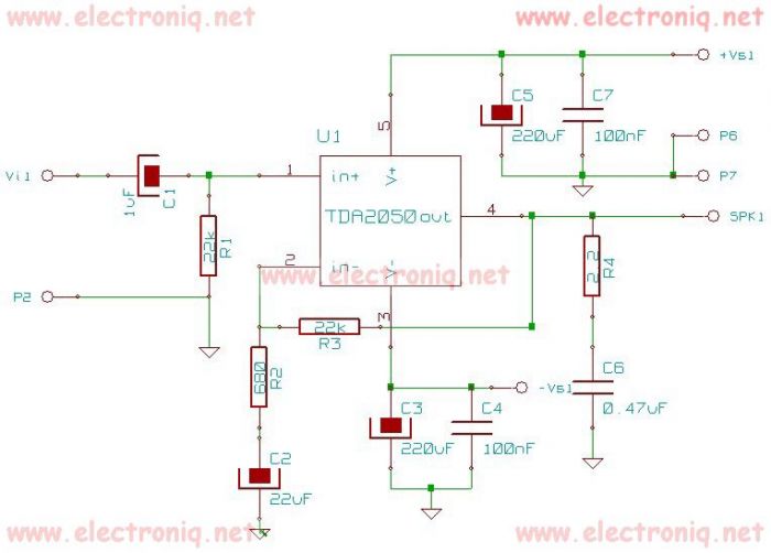
The TDA2050 integrated circuit can be used to design a simple high-fidelity audio power amplifier, intended for use as a Class AB audio amplifier. Due to its high power capabilities, the TDA2050 audio power amplifier can deliver up to...

A careful examination of the amplifier photos reveals that the heatsink on the HY60 near-clone built using the TDA2050A is slightly shorter than that of the original HY60s. This unit is positioned at the rear of the amplifier, creating...
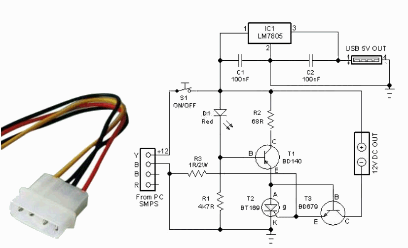
This circuit helps eliminate surplus small AC mains adapters from a desktop. It is a practical DC power supply box powered directly by the SMPS of a desktop PC. The output provides regulated, clean, and protected +12VDC. Additionally, a...
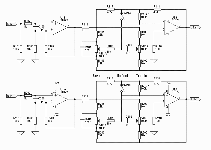
The sound system features a de-sensitized design with a maximum range that can be increased if desired. It includes two tone controls: one offering a lift of 10 dB and the other providing a subtle cut of 3 dB....
The purpose of this report is to provide background and findings of our senior project. We will discuss four steps that we used to complete our final project. The four steps of our project were research and development, design,...
The SSM2306 is a fully integrated, high-efficiency, Class-D stereo audio amplifier designed to maximize performance for portable applications. The application circuit requires minimal external components and operates from a single supply voltage ranging from 2.5 V to 5.0 V....