
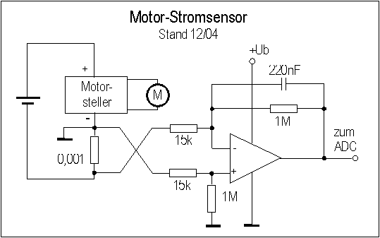
Fast data aquisition 2

The described system is a sophisticated analog multiplexer designed for efficient and accurate signal processing. It utilizes a monolithic architecture that integrates multiple functions into a single chip, which contributes to its low-cost and high-speed performance. The operation begins with the selection of a specific channel, allowing the multiplexer to focus on a particular input signal.
Upon channel selection, the system initiates an analog-to-digital conversion process at a gain of 1. The most significant bit (MSB) of the resulting digital output is crucial for determining the next steps in the conversion process. If the MSB is 1, it indicates that the signal level is within an acceptable range, and the system will proceed to store this value for further processing.
Conversely, if the MSB is 0, this indicates that the signal is below the threshold, prompting the system to increase the gain to 2. This gain adjustment is part of a feedback loop that enhances the system's ability to accurately capture low-level signals. The cycle of gain incrementing, comparison, and conversion continues until an MSB of 1 is achieved, ensuring that the most relevant data is captured.
Once a conversion yields an MSB of 1, the system performs a critical check for an output of all ones, which signifies that the analog-to-digital converter has reached its full-scale output. This condition is essential for verifying the integrity of the conversion process. If the output indicates all ones, the system will then decrement the gain by one step, allowing for a more precise final conversion that reflects the true amplitude of the input signal.
This multiplexer architecture is particularly advantageous in applications requiring rapid signal processing and high accuracy, such as in data acquisition systems, instrumentation, and telecommunications. The iterative gain adjustment mechanism allows for optimal performance across a wide range of input signal levels, making it a versatile component in modern electronic designs.a low cost, high-speed monolithic analog multiplexer. The system works as follows: Selects a channel and initiates a conversion at G = 1 and then looks at the MSB of the conversion result. If the MSB = 1, the ?? will store the value. If the MSB = 0, the ?? will select G = 2. The ?? will repeat the cycle of gain incrementing, comparison, and analog-to-digital conversion until the MSB = 1.
The ?? will then test for an output of all l's, as this is the full-scale output of the A/D. If the output is all l's, the ?? will decrement the gain by 1 step and perform the final conversion.
Related Circuits

Quiz-type game shows are increasingly popular on television. In these games, fastest finger first indicators (FFFIs) are used to test players' reaction times. When a player presses their entry button, their designated number is displayed alongside an audio alarm....
The new data-logger software is not yet completely finished. But the hardware design is frozen and will probably not be changed anymore. The printed circuit board is a bit smaller than the old one (36x22mm). But unfortunately the new...
The image 3-6 depicts a thermistor temperature or frequency conversion circuit. The resistance of thermistors changes linearly with temperature, allowing this change to be utilized in a voltage-controlled oscillator. In the circuit, operational amplifiers A1-A4 are current-type LM3900 models,...
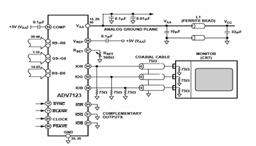
This digital-to-analog converter (DAC) integrated circuit is designed for optimal noise performance, minimizing both radiated and conducted noise. A recommended connection diagram for the ADV7123 is depicted in the following schematic diagram. According to the ADV7123 datasheet, this device...

A data logger is a device that records measurements over time. The measurements could be any physical variable like temperature, pressure, voltage, humidity, etc. This project describes how to build a mini logger that records surrounding temperature. A data logger...
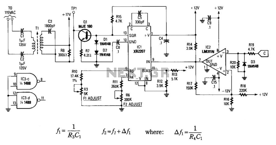
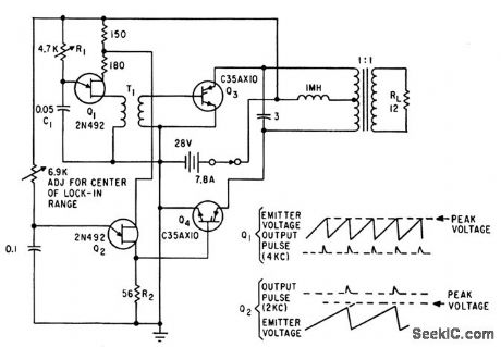
In this circuit, data at input C is amplified by IC2 and then fed to modulator IC1. IC1 generates two frequencies, depending on the values of C5, I10, R5, Rn, and R6. The frequency f1 is generated if pin...