
Fiber-optic-receiver
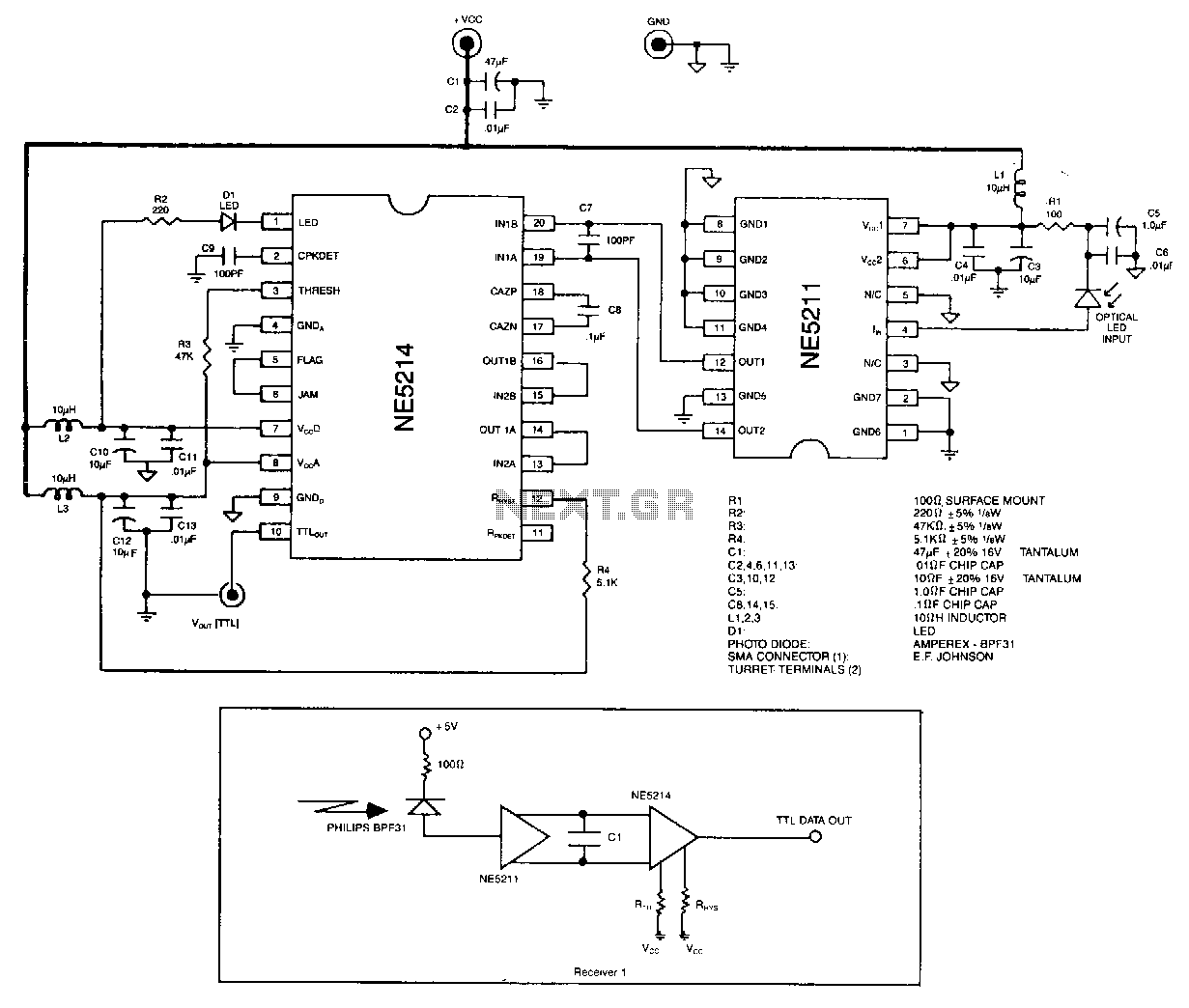
The optical signal is coupled to the pin diode. Current flowing in the diode also flows into the input of the NE5211 preamplifier. The preamplifier is a fixed-gain block that has a 28 kΩ differential transimpedance and performs a single-ended to differential conversion. With the signal in differential form, greater noise immunity is assured. The second stage, or postamplifier NE5214, includes a gain block, auto-zero detection, and limiting. The auto-zero circuit allows decoupling of the preamplifier and the postamplifier and cancels the signal-dependent offset due to the optical-to-electrical conversion. The auto-zero capacitor must be 1000 pF or greater for proper operation. The peak detector has an external threshold adjustment, RTH, allowing the system designer to tailor the threshold to the individual's needs. Hysteresis is included to minimize jitter introduced by the peak detector, and an external resistor, RHYS, is used to set the amount of hysteresis desired. The output stage provides a single-ended TTL data signal with matched rise and fall times to minimize duty-cycle distortion.
The described circuit represents a sophisticated optical signal processing system utilizing a pin diode for initial signal reception. The NE5211 preamplifier serves as the first amplification stage, characterized by its fixed gain and a differential transimpedance of 28 kΩ, which is crucial for converting the single-ended optical signal into a differential format. This conversion enhances noise immunity, a vital feature in high-speed data communication applications where signal integrity is paramount.
Following the preamplification stage, the NE5214 postamplifier further processes the signal. This stage incorporates a gain block that amplifies the differential signal while also integrating auto-zero detection and limiting functionalities. The auto-zero detection mechanism is particularly important as it effectively decouples the preamplifier from the postamplifier, thereby eliminating any signal-dependent offsets that may arise during the optical-to-electrical conversion process.
For optimal performance of the auto-zero circuit, a capacitor with a capacitance of at least 1000 pF is required. This component plays a critical role in stabilizing the system and ensuring that the output remains consistent across varying input conditions. The peak detector within the postamplifier allows for external threshold adjustments via the resistor RTH, enabling customization of the detection threshold to meet specific application requirements.
To mitigate jitter that can be introduced by the peak detection process, hysteresis is incorporated into the design. An external resistor, RHYS, can be adjusted to set the desired level of hysteresis, further enhancing the reliability of the signal detection process.
Finally, the output stage of the circuit is designed to deliver a single-ended TTL data signal. This stage is engineered to ensure matched rise and fall times, which is essential for minimizing duty-cycle distortion. Such precision in timing characteristics is critical for applications involving high-frequency data transmission, where even minor distortions can lead to significant errors in data interpretation. Overall, this optical signal processing circuit exemplifies a well-engineered solution for converting optical signals into reliable electronic data outputs.The optical signal is coupled to the pin diode. Current flowing in the diode also flows into the input of the NE5211 preamplifier. The preamplifier is a fixed-gain block that has a 28-K!J differential transimpedance and does a single-ended to differential conversion. With the signal in differential form, greater noise immunity is assured. The second stage, or postamplifier NE5214, includes a gain block, auto-zero detection, and limiting.
The auto-zero circuit allows de coupling of the preamplifier and the postamplifier and cancels the signal dependent offset because of the optical-to-electrical conversion. The auto-zero capacitor must be 1000 pF or greater for proper operation. The peak detector has an external threshold adjustment, RTH. allowing the system designer to tailor the threshold to the individual"s need. Hysteresis included to minimize jitter introduced by the peak detector, and an external resistor, RHYS. is used to set the amount of hysteresis desired. The output stage provides a single-ended TTL data signal with matched rise and fall times to minimize duty-cycle distortion.
🔗 External reference
Related Circuits
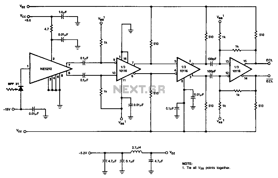
This receiver utilizes the NE5212, the Signetics 10116 ECL line receiver, and the Phillips/Amperex BPF31 pin diode. The circuit is a capacitor-coupled receiver that employs positive feedback in the final stage to introduce hysteresis. The level of hysteresis can...
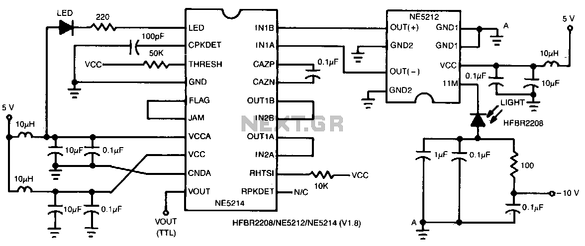
This two-chip receiver, designed for low-cost fiber optic applications at 100-M baud (50 MHz), features a minimal external component count. The receiver consists of pre-amplifier and post-amplifier integrated circuits (ICs) for enhanced stability. The preamplifier IC is characterized by...