
frequency doubler with 4011

The frequency doubler circuit operates by taking an input signal and effectively doubling its frequency through a combination of differentiation and logic gate operations. The inverter (IC1B) plays a crucial role in inverting the incoming signal, which is then processed by the differentiating networks (R1/C1 and R2/C2). These networks are designed to convert the input square wave signal into a series of narrow pulses, thereby facilitating the frequency doubling process.
The NAND gates (IC1A, IC1C, and IC1D) are configured to buffer the signals at various stages of the circuit. IC1A receives the differentiated signal from the networks, while IC1C and IC1D serve to further process the output, ensuring that the signal integrity is maintained throughout the frequency doubling operation. The output of the circuit will exhibit a frequency that is twice that of the input signal, with the pulse widths determined by the values of the resistors and capacitors in the differentiating networks.
This configuration allows for a robust and efficient frequency doubling mechanism suitable for various applications in signal processing and communications. The schematic representation of the circuit, as shown in Figure 2, provides a visual understanding of the signal flow and interactions between the components, highlighting the critical role each part plays in achieving the desired frequency output.This frequency doubler uses one CMOS quad, two input NAND gate package type 4011. The frequency doubler proper consists of an inverter IC1B, two differentiating networks R1/C1, R2/C2 and NAND gate IC1A, IC1C and IC1D function as input and output buffers. In Fig. 2 exist the pulses in different points of circuit. 🔗 External reference
Related Circuits
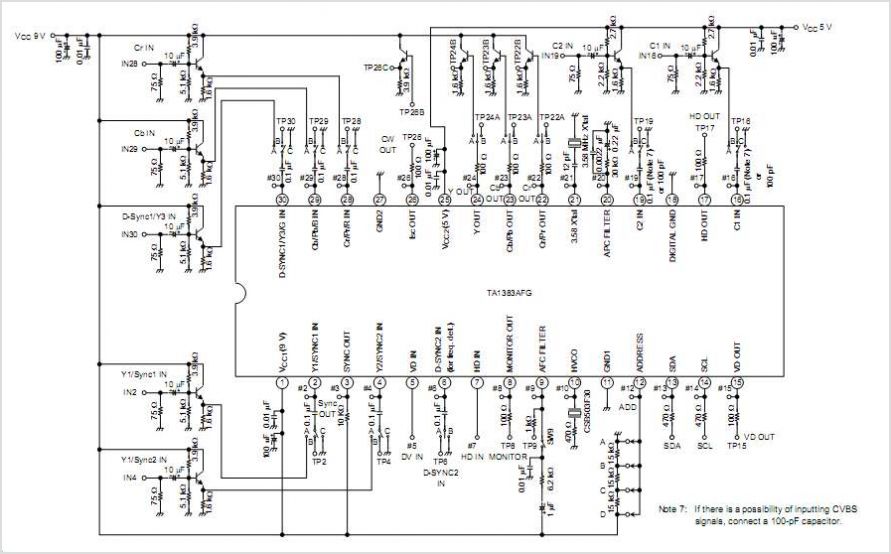
The TA2003PG and TA2003FG are integrated circuits designed for AM/FM radio applications. These ICs facilitate AM/FM radio functionality, including FM front-end and AM/FM intermediate frequency processing. When combined with the TA7368P mono power amplifier IC, a comprehensive AM/FM radio...
Op-amps have been widely used in low-frequency oscillators. Op-amps, or operational amplifiers, are versatile components frequently utilized in the design of low-frequency oscillators. These devices are capable of generating periodic waveforms, such as sine, square, or triangular waves, which are...

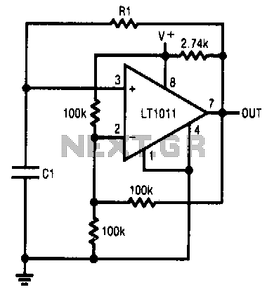
R4 prevents the output voltage from drifting toward one of the supply rails of the operational amplifier. It is understood that R4 should have a high resistance, although the reason for this is unclear. The schematic appears to be...
This simple RC oscillator utilizes a medium-speed comparator with hysteresis and feedback through R1 and C1 as timing elements. The frequency of oscillation is theoretically independent of the power supply voltage. Additionally, the comparator swings to the supply rails...
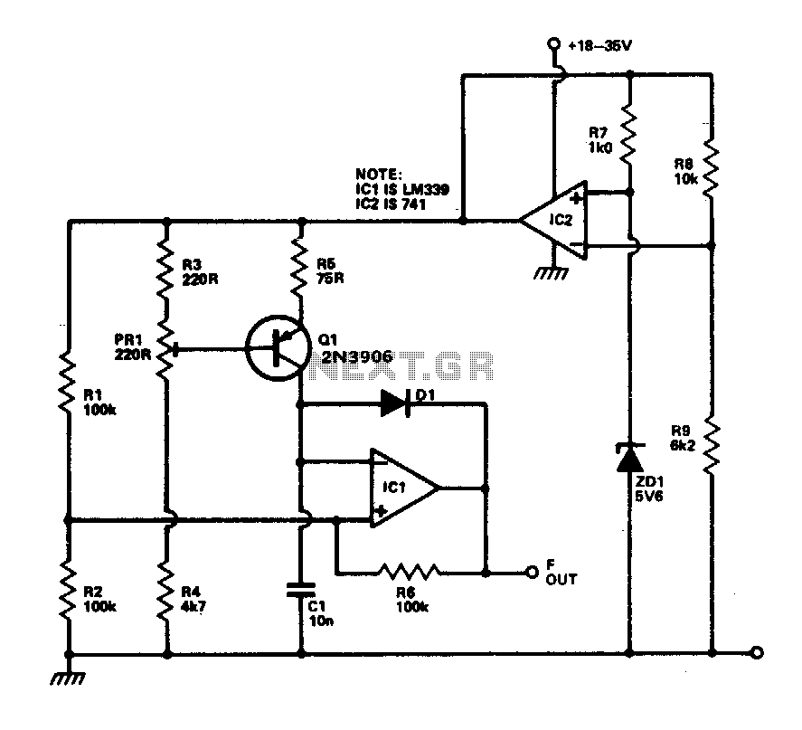
This circuit provides a linear frequency increase of 10 Hz per °C over a temperature range of 0 to 100 °C and can be utilized with logic systems, including microprocessors. The temperature probe Q1, utilizing the Vbe characteristic, changes...

This counter features a four-digit display that can be switched to display frequencies ranging from 1 to 40 MHz, with a resolution of 100 Hz. The MM74C926 CMOS IC serves as the four-digit decimal counter, which can latch a...