
General Purpose Amplifier circuit diagram

The described circuit features a unique configuration that enhances performance by removing external input resistors. This modification significantly minimizes the variability associated with the working point stabilization, allowing for more consistent circuit behavior. The implementation of two DC negative feedback loops serves to further stabilize the circuit's operation, improving linearity and reducing distortion.
In this configuration, the first stage operates as a signal amplifier, where the output is derived from the extreme base. This arrangement ensures that the signal is amplified before being processed by the second stage. The second stage, which follows the first, receives its input from the collector of the first stage. By linking the collector of the second stage back to the emitter of the first stage, the circuit creates a feedback path that enhances stability and linearity.
The use of negative feedback in this circuit is crucial, as it helps to counteract any variations in the output that may arise due to changes in temperature or supply voltage. By continuously feeding a portion of the output back into the input, the circuit can maintain a more stable operational point, leading to improved performance across a range of conditions.
This circuit design is particularly beneficial in applications requiring high fidelity and precision, such as audio amplification or signal processing systems. The elimination of external resistors and the strategic use of feedback contribute to a more reliable and efficient circuit, ultimately resulting in superior performance. Circuit characteristic is the elimination of the external input resistors, thereby reducing the element of the working point stabilization, also uses two DC negative feedback; the second stage exit from the first stage of the extreme base and collector from the second stage to the first stage emitter.
Related Circuits
The diagram illustrates a timed light control switch circuit designed for outdoor advertising light boxes, street lamps, and power control applications in Mexico. This time-saving switch circuit incorporates a manual door switch for controlling the lights, addressing the common...

The Joule thief circuit is well-known among electronics enthusiasts. It has numerous implementations, but the most common is a very minimalist voltage booster. In the simulation file, a 1.5V battery is attached, which is the voltage of a new...

This circuit is beneficial for applications where a load must be activated from one location and deactivated from another. Multiple momentary normally open (N/O) switches or push buttons can be connected in parallel. The circuit described facilitates remote control of...
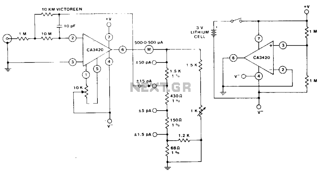
The circuit utilizes the extremely low input current (0.1 pA) of the CA3420 BiMOS operational amplifier. With only one 10 megohm resistor, it achieves a range from ±50 pA maximum to a full-scale sensitivity of ±1.5 pA. Additionally, by...
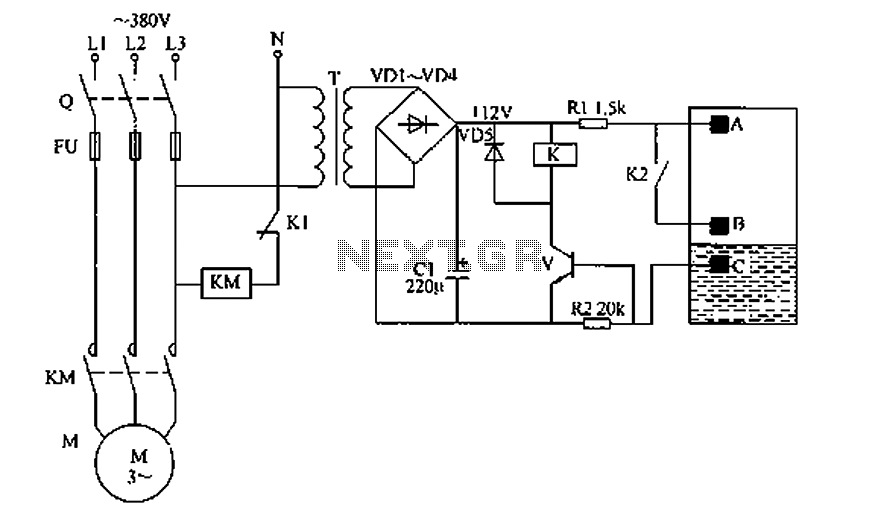
The liquid level automatic controller circuit consists of a power circuit, a level detection circuit, and a control implementation circuit. The power circuit is formed by a power transformer T, rectifier diodes YD1 to VD4, and a filter capacitor...
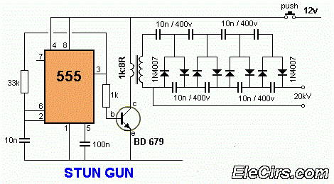
A 12V to 20000V inverter circuit diagram (stun gun) is presented. This circuit generates a very high voltage and must be used with caution to prevent electric shock. The transformer can produce over 1000V and amplify the voltage by...