
Handy Cricket Hardware Description

The Handy Cricket is a compact electronic device designed for educational and recreational purposes, primarily aimed at children. The hardware design incorporates various components that work together to provide an interactive experience. Central to the device is a microcontroller, which serves as the brain, executing programmed instructions and managing input/output operations.
The schematic includes a power supply section that typically consists of a battery or a rechargeable power source, ensuring portability. Voltage regulators may be incorporated to provide stable operating voltages for the microcontroller and peripheral components.
Input mechanisms such as buttons or touch sensors allow users to interact with the device. These inputs are connected to the microcontroller's GPIO (General Purpose Input/Output) pins, enabling the device to respond to user actions.
Output components may include LEDs, speakers, or motors, which provide feedback or perform actions based on user inputs. The schematic would detail the connections from the microcontroller to these output devices, typically through driver circuits to handle the required current and voltage levels.
Communication interfaces, such as I2C or SPI, may be included to connect additional sensors or modules, expanding the device's capabilities. For instance, a Bluetooth module could be integrated for wireless communication, allowing the Handy Cricket to interact with smartphones or tablets for enhanced functionality.
Overall, the hardware design of the Handy Cricket emphasizes simplicity and user-friendliness while ensuring that the device remains robust and versatile for various applications.This document presents an overview of the hardware design of the Handy Cricket. 🔗 External reference
Related Circuits
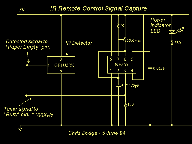
The hardware is constructed from two modules, one to capture the signal and provide timing functions, and the second as transmitter placed somewhere near the target equipment. It has been interfaced with an IBM compatible PC on the printer...

The V2.2 PCB features four spare connectors (X11 to X14) that can be utilized for various inputs and outputs, as they are conveniently accessible on the 37-pin DB connector. Similarly, the V3.0 PCB includes four spare connectors (SPR1 to...
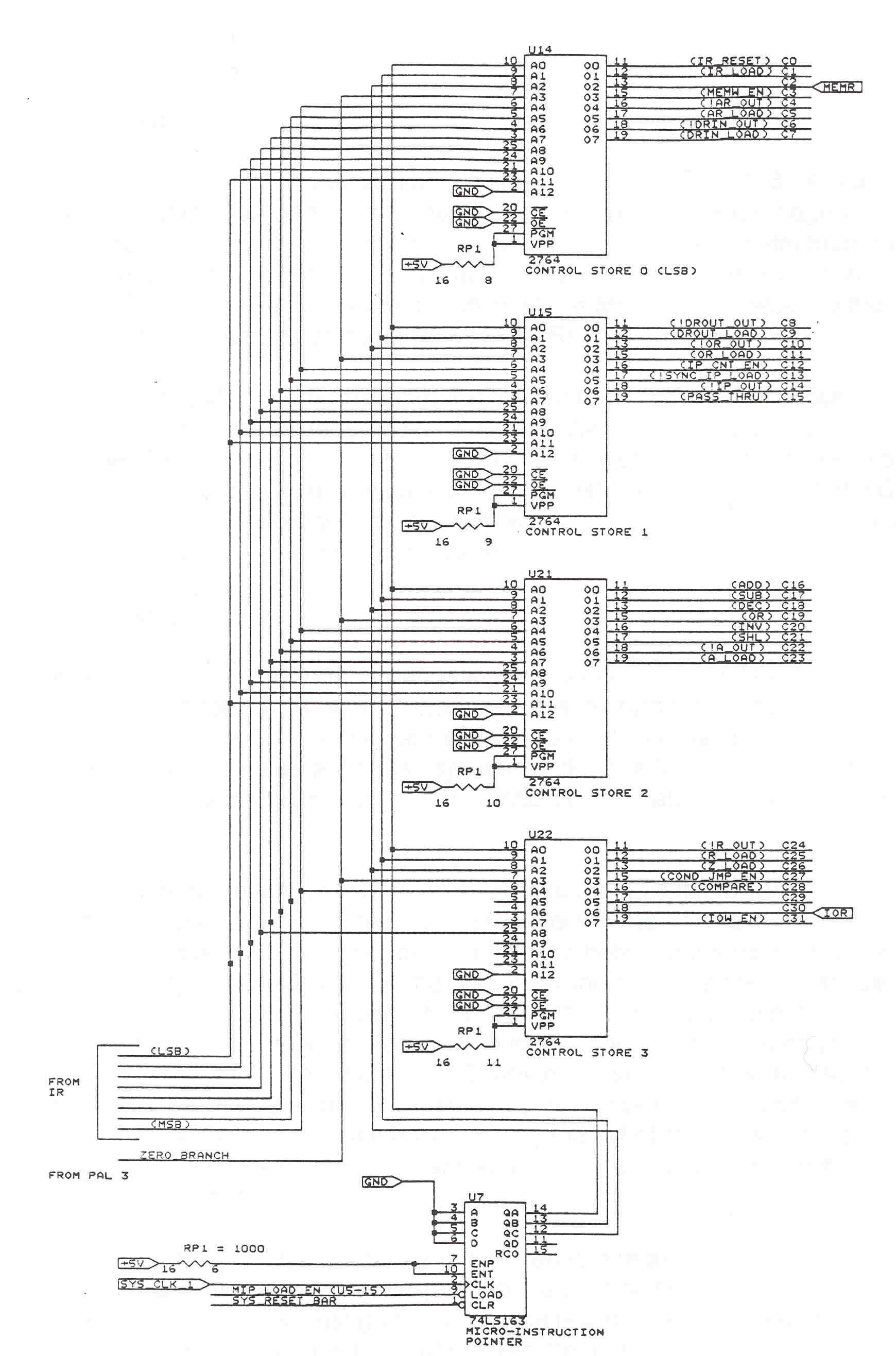
The datapath consists of registers, an ALU, and an internal system bus. Registers are fast memory locations internal to the CPU, distinct from main system memory, and serve as temporary storage during calculations. The ALU is a combinational logic...
When the water level is low, the wires in the tank are open-circuited, and the 180K resistor pulls the switch low, resulting in the switch opening and the LEDs turning OFF. As the water begins to fill the tank,...
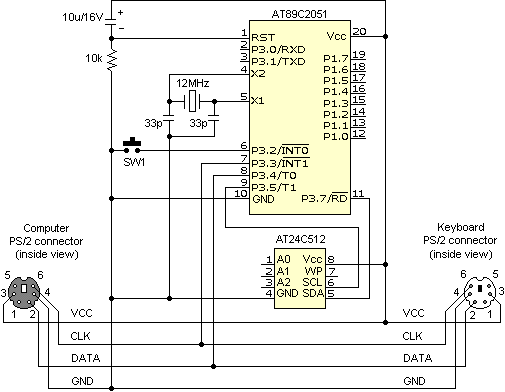
The Atmel AT89C2051 keylogger circuit connects to a PC keyboard via a PS/2 connection cable, facilitating data transfer between the keyboard and the circuit during program execution. The Atmel AT89C2051 microcontroller is a popular choice for implementing keylogger circuits due...
The Openbench Logic Sniffer is an open-source logic analyzer designed to support the SUMP logic analyzer software at minimal cost. Source and design files can be downloaded from the Gadget Factory project page. The project originated from discussions in...