
How to use SPI (Serial Peripheral Interface) in AVR Microcontrollers
 in AVR Microcontrollers")
The Serial Peripheral Interface (SPI) is a synchronous serial communication protocol that facilitates data exchange between a master device and one or multiple slave devices. The architecture of SPI is characterized by its simplicity and efficiency, making it suitable for a wide range of applications, including microcontroller communication with peripheral devices like sensors, memory cards, and display modules.
In an SPI configuration, the master device generates the clock signal, which synchronizes the data transmission on the two data lines, MOSI (Master Out Slave In) and MISO (Master In Slave Out). The master also controls the selection of slave devices through the Slave Select (SS) line, ensuring that only one slave is active during communication. The SPI protocol allows for full-duplex communication, meaning that data can be sent and received simultaneously, increasing the overall throughput of the system.
The SPI bus operates with a minimum of four lines: SCK (clock), MOSI, MISO, and SS. Additional slave devices can be connected to the same bus, each with a dedicated SS line controlled by the master. This configuration allows for multiple slaves to be addressed without the need for complex handshaking protocols, as the master simply toggles the SS line to select the desired slave.
In terms of electrical characteristics, the SPI bus can operate at various clock speeds, determined by the master. The SPI clock frequency (SCK) is critical in ensuring reliable data transfer, and its relationship with the oscillator frequency must be carefully managed, especially in systems with multiple devices operating at different speeds.
The SPI protocol also includes status flags, such as SPIF and WCOL, which provide feedback on the status of data transfers. The SPIF flag indicates the completion of a data transfer, while the WCOL flag indicates a write collision, which occurs if data is written to the SPI Data Register during an active transfer. Proper handling of these flags is essential for robust SPI communication.
Overall, the SPI protocol's straightforward design and high-speed capabilities make it a preferred choice in embedded systems, where efficient communication between microcontrollers and peripherals is essential.SPI stands for Serial Peripheral Interface and it is the simplest among all the communication protocols. 8bit data registers in the devices are connected by wires. These data registers works as shift registers and one of the device controls the data exchange inside the SPI Network.
The device or devices that controls the operation inside the netwo rk is known as the Master. For more elaboration, you may read the Wikipedia article: Serial Peripheral Interface Bus. There can be multiple Masters in a system. There may be multiple slaves too. The slave need not to be another micro controller. It can be an SD card, or some display device or may be some other electronic circuit. Irrespective of the device attached as a slave, it needs to get selected by master device(s) for data transfer. If the system is a multi-master network, then each individual secondary master needs to be selected for mastering the SPI BUS.
An SPI bus consist of two DATA lines, one clock line, and device select (or slave select) lines. The clocking signal is generated by the master in the network. Here, in this experiment, one system is build up to receive any character transmitted in the SPI. And it displays the character on the LCD display. So the receiver circuit is essentially a slave. As the receiver system will never transmit any data, we can keep it enabled all the time. There would be a master device that will transmit a string of character, either once, or repetitively. So let`s see, what are the available resources for this communication. When a serial transfer is complete, the SPIF Flag is set. An interrupt is generated if SPIE in SPCR is set and global interrupts are enabled. If SS is an input and is driven low when the SPI is in Master mode, this will also set the SPIF Flag.
SPIF is cleared by hardware when executing the corresponding interrupt Handling Vector. Alternatively, the SPIF bit is cleared by first reading the SPI Status Register with SPIF set, then accessing the SPI Data Register (SPDR). The WCOL bit is set if the SPI Data Register (SPDR) is written during a data transfer. The WCOL bit (and the SPIF bit) are cleared by first reading the SPI Status Register with WCOL set, and then accessing the SPI Data Register.
When this bit is written logic one the SPI speed (SCK Frequency) will be doubled when the SPI is in Master mode. This means that the minimum SCK period will be 2 CPU clock periods. When the SPI is configured as Slave, the SPI is only guaranteed to work at or lower. This bit selects Master SPI mode when written to one, and Slave SPI mode when written logic zero. If SS is configured as an input and is driven low while MSTR is set, MSTR will be cleared, and SPIF in SPSR will become set.
The user will then have to set MSTR to re-enable SPI Master mode. These two bits control the SCK rate of the device configured as a Master. SPR1 and SPR0 have no effect on the Slave. The relationship between SCK and the Oscillator Clock frequency is shown in the following table: 🔗 External reference
Related Circuits
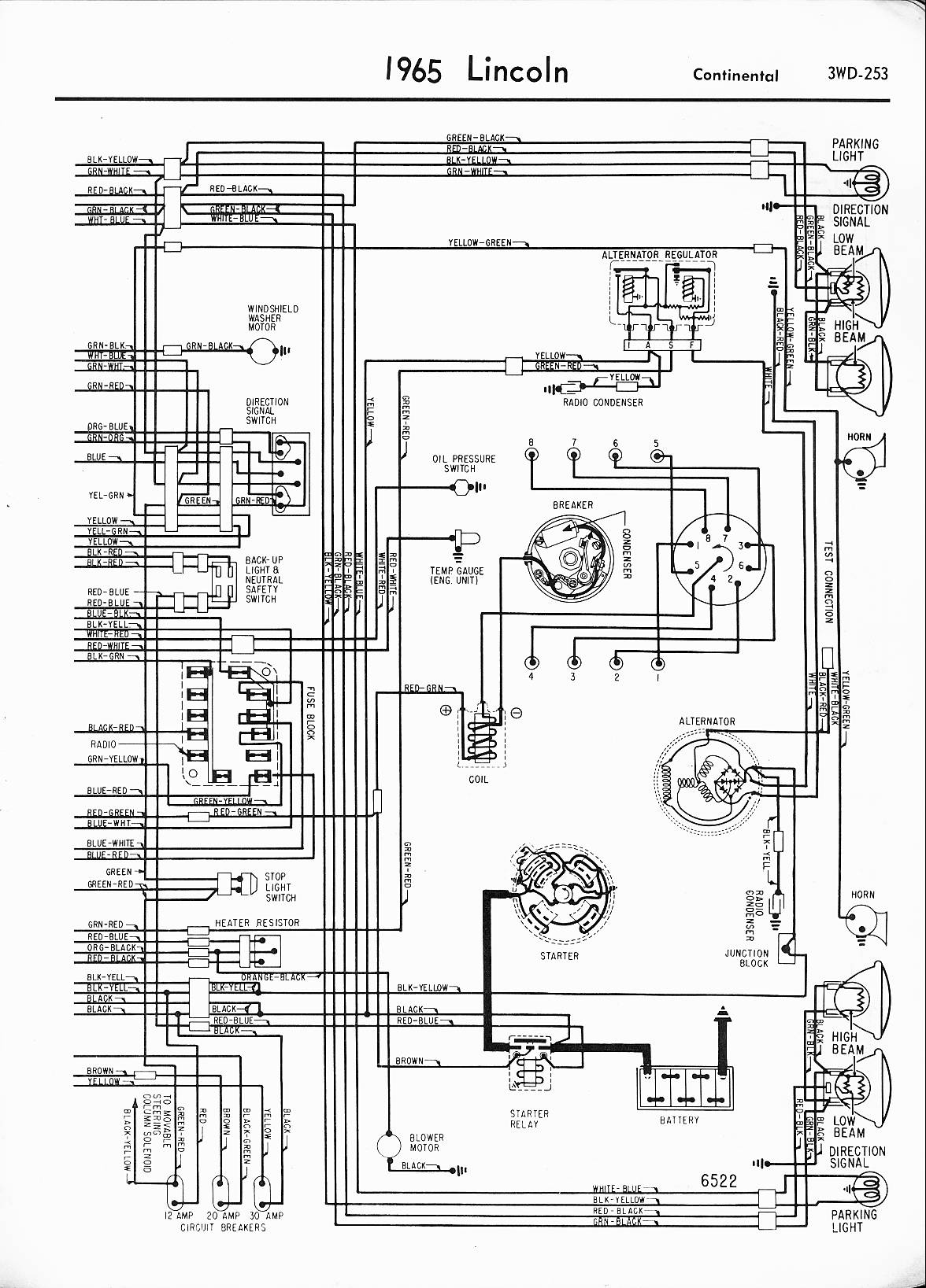
A 1971 Lincoln Continental 4-door is experiencing a complete power failure inside the vehicle, particularly affecting the ignition switch. The battery cables, post connectors, and fusible link have been checked and are functioning correctly. All fuses in the fuse...
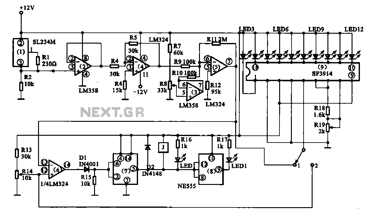
Vegetable greenhouse temperature detection control circuit. The greenhouse temperature detection control circuit is primarily composed of a temperature sensor SL234M, operational amplifiers LM324 and LM358, a dual time base circuit NE555, a relay, and a display driver circuit. The...
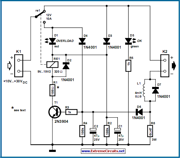
This circuit is particularly beneficial for hobbyists utilizing a breadboard to experiment with ideas, alongside a simple homemade DC power supply comprising a transformer, rectifier, smoothing capacitor, and protective fuse, which lacks overcurrent protection. In this design, resistor R6...
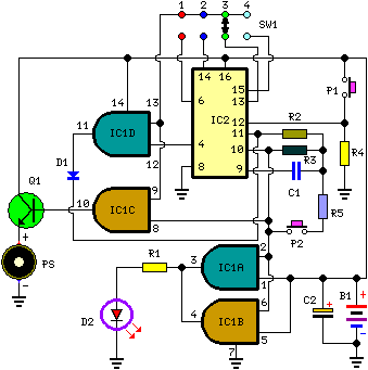
Pressing P1 resets IC2, which then begins oscillating at a frequency determined by R3 and C1. With the specified values, this frequency is approximately 4Hz. LED D2, controlled by IC1A and IC1B, flashes at the same oscillator frequency, indicating...
Atmel's application note AVR109 describes a bootloader that utilizes the UART for communication of FLASH programming instructions. It also provides sample C code that facilitates the programming of FLASH, EEPROM, and lock bits. It is important to note that...

The AT89C family of microcontrollers features a parallel programming interface for flash memory. To write information, a programming voltage of 12V is required, and nearly all pins of the ports are utilized for this purpose. Consequently, parallel programming is...