
Inverting monostable circuit diagram

The timer 555 is a versatile integrated circuit commonly used in various timing, delay, and oscillator applications. In a typical configuration, the 555 timer operates in either monostable or astable mode, depending on the desired output behavior. When triggered by a positive pulse at the trigger pin (pin 2), the timer transitions from its low state to a high state, producing a negative output pulse at the output pin (pin 3). This output pulse duration is determined by the external resistors and capacitors connected to the timer.
In applications where the duty cycle is maintained above 99%, the timer can effectively handle heavy loads connected to pin 7, which is the discharge pin. This feature allows for the separation of heavy loads from the timing components without compromising the accuracy of the timing cycle. However, care must be taken when loads exceed the specifications related to pin 3, as excessive loading can lead to inaccuracies in the timing intervals.
To ensure optimal performance, it is essential to select appropriate resistor and capacitor values to establish the desired timing characteristics while considering the load requirements. The 555 timer can be used in various circuits, including pulse-width modulation (PWM) applications, frequency generation, and timer circuits, making it a fundamental component in electronic design. Proper understanding of the connections and behavior of the 555 timer is crucial for achieving reliable and precise operation in diverse applications. As shown in the timer 555 is triggered by the positive trigger pulse, then a negative output pulses. In the absence of beating duty cycle greater than 99%. Heavy loads can be s eparated from the pin 7, will not affect the accuracy, but will affect the load exceeds 3 pin timing accuracy.
Related Circuits
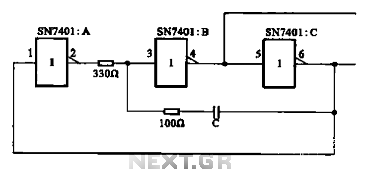
The clock signal generating circuit utilizes an RC configuration, commonly applicable in most TTL systems. This circuit requires a set of six inverters, specifically three inverters from the SN7401 series. The clock frequency is determined by the values of...
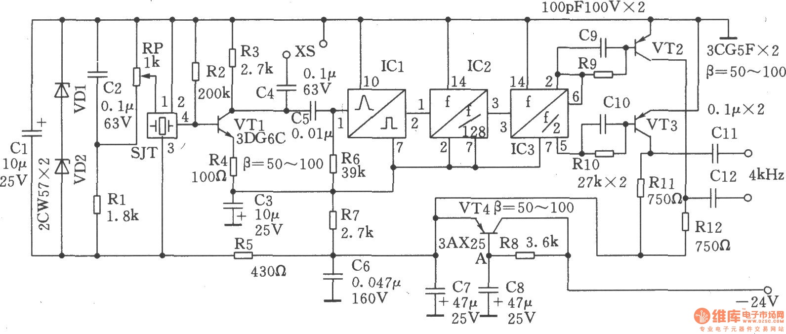
The circuit SJT is a 1024 kHz warming crystal oscillator. The circuit is illustrated in the accompanying chart. Due to the low output signal level, a transistor (VT1) is employed as a buffer amplifier. The base bias resistor (R2)...

The protected section of track can be of any desired length and does not need to be equal on both sides of the crossing. The circuit operates bidirectionally and can be linked with other grade crossing circuits to provide...
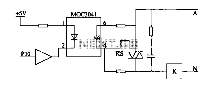
Device for an intermediate relay. The circuit utilizes a Triac AC contactor interface, employing the MOC3041 Triac output optical coupler to trigger the Triac. When Pl0 is low, the Triac will be activated, energizing the AC contactor coil. The described...

The 78W series voltage regulators are designed to handle an input voltage of approximately 35V, while the 24V type can withstand up to 40V. It should be noted that these regulators will not operate effectively with a significant input-output...
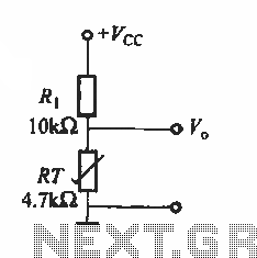
The basic application circuit for thermistors is illustrated. Figure (a) depicts a fundamental temperature measurement circuit. The accuracy of this temperature measurement is not high and is suitable only for applications with lower precision requirements. RT represents a positive...