
LCD_controller

The clip sync output to TTL level appears to require additional time to accommodate extra components on the board. As a temporary solution, a ZPD4.7 (4.7 V Zener Diode) should be placed between SG and ground at the power switch (ring to SG), along with a 1k resistor connecting the SG output from the BOTPCB to the SG pad of the power switch to clip SYNCOUT to 4.7V. This controller is primarily based on the circuit designed by Thomas Schuhmann and Franz Krause. Several improvements and simplifications have been incorporated, drawing inspiration from contributions in the homebrew section at stereo3d.com. The PLL circuit has been fine-tuned to reduce jitter, with a frequency multiplication circuit modified to operate within a narrower frequency range of approximately 25 to 300 Hz, ensuring stability at typical V-sync frequencies (~100 Hz). The circuit automatically adapts the generated V-Sync polarity, converting the received V-sync signal to a positive polarity while maintaining synchronization with the generated signal, regardless of the original pulse polarity. The design effectively combines features for driving shutter glasses, utilizing a flip-flop to toggle the polarity of the glasses at half the L/R switching frequency, similar to the original Cyberboy controller but without requiring an additional negative supply voltage. Instead, the common line for both LCDs is driven in reverse to the currently active LCD, as implemented in the standard 4070 homebrew driver. EAGLE CAD users can download a ZIP archive containing the EAGLE sources for the circuit schematics and PCB layout. It is recommended to use a picture editor to adjust the PCB layout to the printer's resolution. For PCB fabrication, the layout can be printed on a laser printer and transferred using a toner transfer method. The PCB design consists of two interconnected boards, with specific drilling requirements for component mounting.
The circuit design is characterized by its adaptability and efficiency, particularly in synchronizing V-sync signals for display applications. The integration of a Zener diode serves as a voltage clamp, ensuring that the SYNCOUT signal remains at a safe TTL level, thus preventing potential damage to downstream components. The use of a 1k resistor in conjunction with the Zener diode helps to limit the current flowing through the diode, enhancing the reliability of the circuit.
The PLL (Phase-Locked Loop) circuit is a critical component of this design, as it stabilizes the frequency of the output signal. By narrowing the frequency range to 25-300 Hz, the circuit minimizes jitter, which is essential for maintaining a clear and stable image on the display. This adjustment reflects a thorough understanding of the interplay between frequency stability and image quality, particularly in applications that rely on precise synchronization.
The automatic polarity adaptation feature is particularly noteworthy, as it allows the circuit to accommodate various V-sync signal types without manual intervention. This capability enhances the usability of the design, making it suitable for a wider range of applications. The flip-flop integration for shutter glasses operation is another innovative aspect, allowing for efficient control of the glasses without the need for additional power supplies.
In terms of physical design, the dual PCB structure facilitates a compact layout while enabling effective heat dissipation and component accessibility. The specific drilling requirements ensure that components are securely mounted, with careful consideration given to the placement of connectors and switches for user interaction.
Overall, this circuit design exemplifies a well-thought-out approach to electronic engineering, incorporating both innovative features and practical solutions for real-world applications. The availability of EAGLE CAD files further supports the community-driven aspect of the project, allowing others to replicate or modify the design as needed.Clip sync output to TTL level seems to take some more time to fit the extra parts on the board; as a quick fix, put a ZPD4. 7 (4. 7 V Z-Diode) between SGand ground at the POWERswitch (ring to SG) and a 1k resistor between the SGoutput from the BOTPCBand the SGpad of the power switch to clip SYNCOUTto 4.
7V : This controller is based mainly on the c ircuit by Thomas Schuhmann & Franz Krause. I added some improvements and simplifications (which I may have seen in other circuits, so credits go to all those nice people that contributed to the homebrew section at stereo3d. com ). PLL circuit fine-tuned for less jitter - Thomas once told me that he just used an out-of-the-box circuit for frequency multiplication, which had a far too wide frequency range (~10 kHz) to be really stable at usual V-sync frequencies (~100 Hz).
I restricted the range to approx. 25. 300 Hz and get a rock-steady picture now. Automatic adaptation of generated V-Sync polarity. The original circuit didn`t care for the polarity (positive or negative pulses) of the V-sync signal, but always synchronize to the rising edge of the pulse. My circuit automagically converts the received V-sync signal to positive polarity, and the generated sync signal back to the received polarity, keeping the first edges of received and generated signal in sync regardless of polarity.
Combines `the best of both worlds` w. r. t. shutter glasses driving: Like the original Cyberboy controller, I use a (spare from the sync-doubler) flip-flop to get half of the L/R switching frequency to toggle the polarity of the glasses (in contrast to the extra oscillator in the standard 4070-homebrew driver). Unlike the Cyberboy, however, I don`t use an additional negative supply voltage, but instead drive the common line for both LCDs reversed to the currently active LCD (as in the standard 4070-homebrew driver).
If you already own (or are willing to download the 4 MB free light/evaluation version of) EAGLE CAD, you can download a ZIP archive with the EAGLE sources for the circuit schematics and PCB layout Since I don`t know your printer, you will have to use a picture editor like Picture Publisher, MS Photopaint etc. to convert the PCB layout to your printer`s resolution. I`ve had cases where the editor assumed a resolution of 96 dpi, which would give a ridiculously large image.
If you have (access to) a laser printer, just print the layout as it is (i. e. mirrored) and iron the laser toner onto the (clean) copper side of the PCB. Then soak the paper with warm water until you can gently peel and rub it off until (almost) only the laser toner remains on the PCB. For best results, print at least twice on the same page to get an extra thick toner layer (although it will be hard to get the prints exactly in the same place).
Normal printer paper (kind of) works, but may leave some paper fibres. I also tried coated Hi-Res inkjet paper, which seems to have finer fibres, but only does a little better job. If you are used to make PCBs by photo-transfer, just print the board layout in original size on a sheet of overhead projection film (as recommended for your printer) and expose as usual (printed side to the PCB, so you can read the text).
Having etched the PCB, cut out the two parts along the inner thin lines. I had to cut out the lower left corners to get around the screw that holds my case together - that`s why the black rectangles are there. Drilling : 1. 5mm for 3. 5mm jack pins (4 holes, base pin bent around PCB edge), 0. 8mm for all others. Enlarge holes for IC socket pins to 1. 5mm on the components side ( see below) ; put board on a metal plate to avoid drilling through the copper film.
The circuit is designed to consist of two PCBs, with the smaller one mounted on top of the other, connected by 5 vertical wires, five external switches and an external LED. (if you`re very brave) solder the chips directly to the PCB. In this case, some 🔗 External reference
Related Circuits
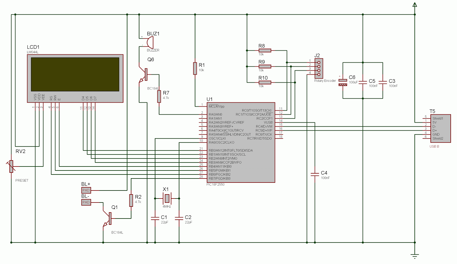
This project involves a USB interface for an alphanumeric LCD display, such as the 4x20 model, which can be controlled using the LCD Smartie program. The USB interface is implemented with the PIC18F2550 microcontroller and utilizes USB LCD modules....