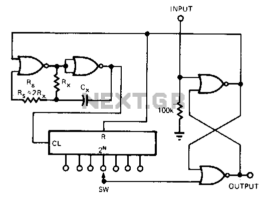
Low-power-wide-range-programmable-counter

This CMOS circuit functions as a one-shot time delay switch and a general-purpose timer. It comprises a gated oscillator and a latch utilizing a CD4001 quad 2-input NOR gate, along with a CD4020 14-stage counter. The timing interval, TON, is determined by the oscillator frequency, which is influenced by the resistor-capacitor (RxCx) combination and the appropriate output from the counter. A pulse applied to the latch activates the oscillator and counter. The output from the latch remains high until the 2N count resets the latch, subsequently disabling the oscillator and counter. This circuit is capable of providing timing intervals ranging from milliseconds to hours. The exceptionally long durations achievable with the CMOS oscillator, in conjunction with the 14-stage counter, facilitate this extensive range. Additional decoding is necessary for timing variations that are finer than a power of two.
The circuit operates by leveraging the characteristics of CMOS technology, which allows for low power consumption and high noise immunity. The CD4001 quad 2-input NOR gate serves as the primary building block for the latch, which is essential for maintaining the state of the oscillator and counter. The configuration of the gated oscillator generates a clock signal whose frequency is determined by the external resistor-capacitor network (RxCx). This clock signal is fed into the CD4020 counter, which counts the pulses generated by the oscillator.
When a pulse is applied to the latch, it enables the oscillator and starts the counting process. The latch output remains high, indicating that the circuit is active. The counter continues to increment until it reaches a predetermined count of 2N, at which point it resets the latch. This reset action disables both the oscillator and the counter, effectively ending the timing interval.
The timing capability of this circuit is particularly versatile, allowing for a wide range of applications, from simple delay functions to more complex timing scenarios. The use of a 14-stage counter expands the timing range significantly, making it suitable for applications requiring long delays or timing intervals. For applications that necessitate finer timing resolutions, additional decoding circuits can be integrated to achieve precise timing adjustments.
In summary, this CMOS circuit design is an efficient solution for implementing time delay switches and timers, utilizing fundamental digital logic components to achieve reliable performance across a broad spectrum of timing applications.This CMOS circuit can be used as a 1-shot time delay switch and general-purpose timer. The circuit consists of a gated oscillator and a latch made from one CD4001 quad 2-input NOR gate as shown and a CD4020 14-stage counter. TON is a function of the oscillator frequency from the RxCx and the proper zN output from the counter.
A pulse applied to the latch will "enable" the oscillator and counter. The latch output will remain high until the 2N count resets the latch and disables the oscillator and counter. The circuit provides flS to hour interval timing. The extraordinarily long periods available from the CMOS oscillator, combined with the 14-stage counter, make this range possible. Further decoding is required for variations finer than a power of two.