
low ripple regulated power supply

The schematic involves a configuration where capacitor C2 plays a crucial role in filtering and stabilizing the output voltage of the circuit. The transistors Q1 and Q2 are typically configured in a common-emitter or common-collector arrangement, where their gains are pivotal in determining the overall performance of the circuit. The combined gain of these transistors influences the effective capacitance seen at C2, enhancing its role in smoothing out voltage fluctuations.
In practical applications, selecting a larger capacitance value for C2, such as 100 µF, can significantly improve the transient response of the circuit, allowing it to better handle variations in load and input conditions. The minimum hef values for Q1 and Q2 should be carefully considered, as they will directly affect the circuit's stability and response time. Proper biasing of the transistors is essential to ensure that they operate within their optimal ranges, thus maximizing the effectiveness of C2 in achieving the desired smooth output.
Additionally, the choice of C2's value should take into account the operating frequency of the circuit. Higher capacitance values may introduce delays in response time, which could affect high-frequency performance. Therefore, a balance must be struck between the desired smoothness and the dynamic response of the circuit, ensuring that the selected capacitance aligns with the overall design objectives.C2 can be chosen for the degree of smoothness as its value is effectively multiplied by the combined gains of Q1/Q2, if 100 µF is chosen for C2, assuming minimum hef for Q1 and Q2, 🔗 External reference
Related Circuits

The concept of distributed active RIAA correction and the use of negative feedback to linearize the input stage is appealing. However, the original design by Collin has significant flaws, including poor power supply rejection ratio (PSRR) in the input...
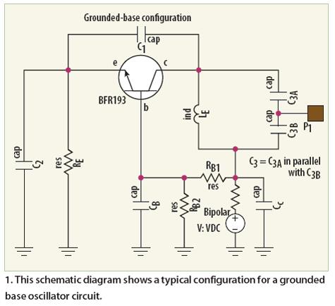
Unlike conventional small-signal methods, employing large-signal, time-domain design techniques facilitates the development of low-noise grounded-base oscillators suitable for VHF/UHF applications. The implementation of large-signal, time-domain design techniques in the creation of grounded-base oscillators represents a significant advancement in the field...
Power line fluctuations and cut-offs can damage electrical appliances connected to the line, particularly domestic appliances such as refrigerators and air conditioners. When a refrigerator operates at low voltage, excessive current flows through the motor, leading to overheating and...
The NE568A (NE568AD, NE568AN, SA568AD, SA568AN) is a monolithic phase-locked loop (PLL) that operates from 1Hz to frequencies exceeding 150MHz. It features an extended supply voltage range and a lower temperature coefficient of the VCO center frequency compared to...
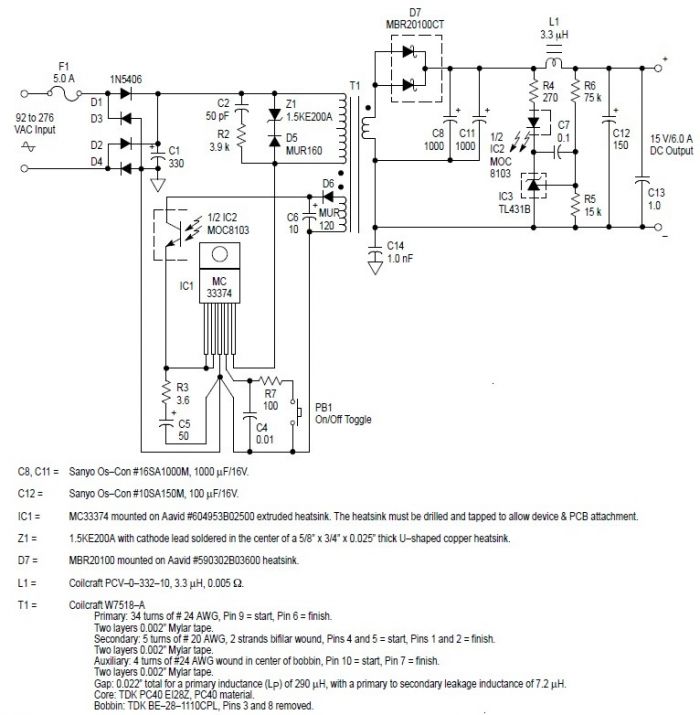
This switching power supply circuit diagram is based on the MC33374 high-power voltage switching regulator IC manufactured by Motorola Semiconductor. The MC33374 switching power supply circuit will provide a maximum output power of around 90 W and requires few...

This simple circuit is designed to provide an output power of approximately 1 watt when connected to a 9-volt power supply. The key advantage of this circuit is its use of a dual Darlington configuration, which increases the input...