
Low Voltage 2mhz Step-up Dc/dc Converter

The AAT1275 evaluation board is designed to facilitate the assessment of the AAT1275 switching boost converter, which is particularly valuable in applications requiring efficient power conversion from low voltage sources. The board's compact design is optimized for portable applications, making it suitable for integration into various consumer electronics.
The evaluation board operates effectively within an input voltage range of 2.7V to 5V, allowing it to accommodate a variety of power sources. A key feature of this design is its ability to provide a stable 5V output voltage capable of delivering up to 500mA of load current, which is essential for USB VBUS operation. The selection of external components is critical; they are chosen not only for their size but also for their performance characteristics, ensuring that the converter operates with high efficiency and minimal output noise.
The TSOPJW-12 package encapsulates the AAT1275, providing a compact footprint while ensuring thermal performance is maintained. The layout of the evaluation board is meticulously designed to minimize parasitic inductance and resistance, which contributes to the overall efficiency of the boost converter.
The evaluation board includes a resistor divider network (R2, R3) that allows for the adjustment of output voltage levels, enabling flexibility in various applications. Additionally, the load switch current limit at OUT2 is set by RSET (R4), providing a safeguard against excessive current draw. This feature is particularly important for protecting the circuit from potential damage due to overload or short circuit conditions. When the current at OUT2 exceeds the predefined limit, the AAT1275 automatically enters a shutdown mode, effectively minimizing power dissipation and reducing stress on the components.
Overall, the AAT1275 evaluation board is a robust platform for evaluating the performance of the AAT1275 boost converter, offering essential features and flexibility for a wide range of applications in portable electronics.The AAT1275 evaluation board provides a platform for test and evaluation of the AAT1275 switching boost converter with USB Power Switch The evaluation board demonstrates suggested size and placement of external components to achieve 5V output voltages and up to 500mA output load current to support USB VBUS operation from an input supply as low as 2. 7V. The external components are selected for small size to suit portable applications while the layout has been optimized to achieve high efficiency and low output noise with the TSOPJW-12 package. The design operates across an input voltage range from 2. 7 to 5V. This document provides details on the operation and test of the AAT1275 Evaluation Board. Modification of the resistor divider network (R2, R3) allows different output voltages. The load Switch current limit level at OUT2 is determined by RSET (R4) value (see Table 1). When the OUT2 pin load current has exceeded current limit level the AAT1275 shuts down to minimize the power dissipation and component stresses under over load and short circuit conditions.
🔗 External reference
Related Circuits
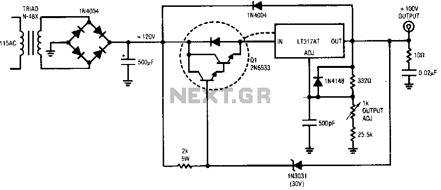
The regulator provides a 100 V output at 100 mA and can withstand shorts to ground. Even at a 100 V output, the LT317A operates in normal mode, maintaining a 1.2 V difference between its output and adjustment pin....
A step-up converter followed by an LDO regulator provides improved battery life compared to a traditional SEPIC design when powered by a single lithium-ion cell. The circuit design features a step-up (boost) converter that elevates the input voltage from a...
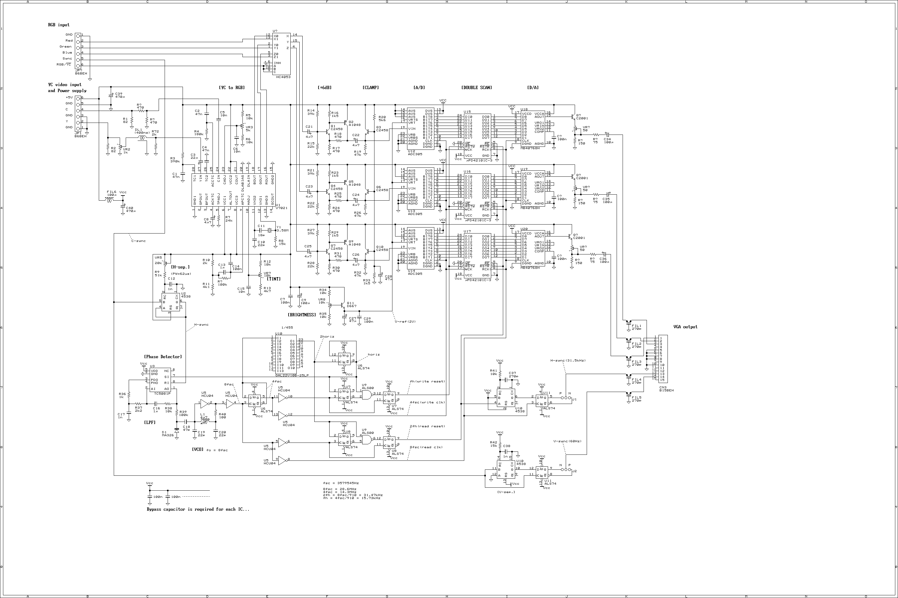
This is a video scan converter to display NTSC video signal into VGA monitor. Normally, the VGA monitor occupies most desk top space, so that everybody will be thinking that if the VGA monitor can be used for video...

A stable voltage source can be generated by amplifying a stable voltage reference. The LM10 component provides both the reference and the amplification. The LM10 is a precision voltage reference and amplifier integrated circuit that is designed to produce a...
All miniature electronic devices operate off batteries. Some of them require higher than the standard battery voltages for efficient operation. If a battery with the specific voltage is unavailable, additional cells must be connected in series to increase the...
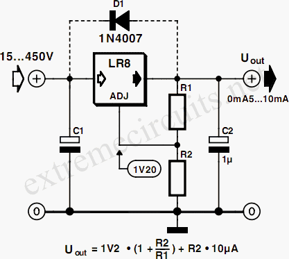
Commonly used 3-pin linear voltage regulators, such as the LM317, cannot handle input voltages exceeding approximately 30V. The LR8A from Supertex Inc is a new adjustable three-pin regulator capable of accepting input voltages up to 450V and supplying an...