
markII
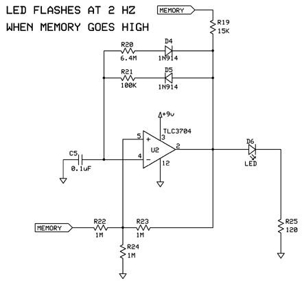
The following circuits are presented in a logical order from initial power-up to the additional features incorporated at the end of the project. A less organized version of the Mark II design exists, but this is the sanitized and organized version. General changes since the Mark I include a switch to 9-volt operation, allowing the use of a single battery that fits in the 9V battery compartment of the chosen enclosure, and a switch to a TLC3704 voltage comparator chip, which is a low-power CMOS alternative to the LM339, rather than the LM324 op-amp. One significant improvement over the Mark I is the implementation of a mechanism to disconnect the batteries when the phone is not in the system, conserving battery power when not in use. To prevent accidental triggering of the detector during the initial power-up phase, when capacitors are charging and the photoresistor is stabilizing, a design consideration ensures that no drastic actions occur for a few seconds after power is applied. This is achieved by keeping the reset pin of the 555 timer low during power-up. Both the Mark I and Mark II circuits function by detecting when the phone display activates, which occurs during incoming calls. While the circuits are similar, the Mark II uses the TLC3704 chip, and an important addition is resistor R8, which provides hysteresis in the circuit to prevent accidental triggering after the photoresistor has been illuminated and is returning to a dark state. The value of R8 was adjusted from an initial 100K to a final 390K to reduce feedback and improve reliability. Initially, various notification methods were considered for when the phone lights up, but the design ultimately settled on simulating a push of a wireless doorbell button. As the button does not need to be pressed for an extended period, the timing components were modified to allow for approximately 0.3 seconds. The reset pin is also where the new power-up delay circuit connects. The Mark II introduces new features utilizing the unused comparators in the TLC3704. A notable addition is a mechanism to indicate if a call was received while away. This is accomplished with a single-bit memory configured with transistors to create a flip-flop, which is set by the output of the 555 timer. One of the TLC3704 comparators is used to drive the memory output line based on the flip-flop's state. An earlier design using the LM339 was adapted, but feedback from the output did not function correctly with the TLC3704 due to the high power-up state of the outputs, which caused the circuit to activate immediately upon power-up. The second part of the missed call notification is a flashing LED that activates when...
The circuit design incorporates several key components and considerations that enhance its functionality and efficiency. The transition to a 9-volt power supply simplifies the power requirements, allowing for a single battery solution. The TLC3704 voltage comparator is crucial for low-power applications, making it suitable for battery-operated devices. The addition of hysteresis through resistor R8 is essential for stabilizing the detection circuit, thereby preventing false triggers during transitional states of the photoresistor.
The 555 timer plays a pivotal role in managing the timing aspects of the circuit. By holding the reset pin low during power-up, the design ensures that the circuit remains inactive until all components are stable, thus avoiding unintended activations. The decision to simulate a wireless doorbell button press for notifications is practical, allowing for a simple yet effective means of alerting the user to incoming calls.
The implementation of a flip-flop memory circuit serves as an innovative solution to retain the state of call notifications, effectively utilizing the additional comparators available in the TLC3704. This approach not only maximizes the use of available components but also enhances the overall functionality of the device. The design considerations taken to adapt the circuit for compatibility with the TLC3704 demonstrate a thorough understanding of component behavior and circuit dynamics, ensuring reliable operation under various conditions.
The flashing LED serves as a clear visual indicator for missed calls, providing immediate feedback to the user. Overall, the Mark II circuit design reflects a thoughtful integration of components, addressing the limitations of the previous version while introducing new features that enhance usability and performance.The following circuits are presented in a logical order (unlike the way they were designed) from initial power-up to the frills tacked onto the end of the project. A less organized and more stream of consciousness version of the Mark II design can be found here, this is the sanitized and organized version.
Some general changes since the Mark I include the switch to 9 volt operation (so I can just use a single battery which fits in the 9V battery compartment of the box I decided to use) and the switch to a TLC3704 voltage comparator chip (a very low power CMOS version of an LM339) instead of a LM324 op-amp. One of the (obvious once I finally thought of it) improvements over the Mark I was the change to actually disconnect the batteries when I don`t have the phone in the system, thus saving lots of battery power while I`m not at home and the phone isn`t in the Mark II.
To prevent accidental triggering of the detector during the initial power-up period when capacitors are charging and the photo resistor is stabilizing, I needed to make sure nothing drastic happens for a few seconds after the power comes on. This circuit does that by holding the 555 timer reset pin low while powering up. The Mark I and Mark II both operate by noticing when the phone display lights up (which happens on incoming calls).
The circuits are fairly similar in both, but I`m using the TLC3704 chip now, and one important change was the addition of resistor R8 to provide some hysteresis in the circuit so it doesn`t accidentally trigger after the photo resistor has already been lit up and is now going back to dark. (I also needed to tweak R8 a little - after everythng was together I found the detector failed intermittently and decided I was getting a little too much feedback.
The 390K value here is the final version and works much better than the initial 100K value I used in the original design). I had all kinds of plans for different things to use for notification of the phone lighting up when I was planning the Mark I, but eventually settled on simulating a push of a wireless doorbell button.
Since that is what I`m also doing in the Mark II, there is no need for the button to be pushed for very long, so the timing components were adjusted to give about 3/10ths of a second. The reset pin here is also where the new power-up delay circuit connects. Now we enter brand new territory for the Mark II. The fact that the TLC3704 had 4 comparators and I was only using 2 of them led me to seek out wacky new features I could add to use up the other two comparators.
One obvious feature missing from the Mark I was a way to know if a call came in while I was gone. The first thing I need is a way to remember that single bit of information, so here is a single bit of memory implemented with some transistors to make a flip-flop (which is set by the output from the 555 timer) and one of the TLC3704 comparators to drive the memory output line from the state of the flip-flop. I had a simpler circuit when I was using the LM339, which I adapted from the "or-gate" sample in the National Semiconductor spec sheet, but feeding back the output as one of the inputs didn`t work for the TLC3704 (apparently the power up state of the outputs is high, so the old circuit immediately turned on at power up).
Continuing the new circuitry, the second part of missed call notification is (obviously) a flashing LED that comes on whe 🔗 External reference