
Mk1 Schematics

The described circuit encompasses a sophisticated design tailored for a microcontroller system, integrating various components to facilitate efficient data processing and communication. The use of 28-pin sockets for RAM chips allows for flexibility in memory selection, accommodating both the 6116 and 6264 RAM types. The LS157 multiplexers play a crucial role in managing control signals, enabling the system to switch configurations as needed. The jumper settings provide versatility, allowing the system to adapt to different operational requirements.
The design emphasizes systematic testing and verification, with a focus on ensuring that each connection is functional before final assembly. The choice of using a hex tri-state inverter for gating signals demonstrates a thoughtful approach to managing data flow, although adjustments were necessary to accommodate the stability requirements of the multiplexer inputs.
The transition from x1 to x16 and x64 modes for UART operation highlights the importance of signal integrity in high-speed communication. The decision to limit the operational modes to those that ensure reliable reception underscores the necessity of robust design practices in electronic circuit development. The use of a 2.4576 MHz crystal to achieve the desired baud rate reflects an understanding of frequency selection in relation to communication protocols.
Overall, this circuit design showcases a blend of innovative engineering and practical problem-solving, resulting in a reliable and efficient system for data handling and transmission.This is an excellent piece of software. It is very easy and enjoyable to use. It comes with a huge library of symbols and also has a library editor for creating your own. I completed all the drawing before a single joint was soldered. This gave me confidence that everything was covered. Ticking off the connections as I went, wiringwas a stress-free no-brainer. Afterwards, I buzzed-out every connection and, again, ticked them off as I went. The original diagrams are in vector format and can thus be scaled to any desired size. In converting them to GIF for the web, I selected a width of 1000 pixels. Download the original hi-res schematics here. I used 28 pin sockets for the RAM chips with a jumper to select 6116 or 6264. I fitted the former but thought it best to support both because the 6116 is hard to source now. The cards also have LS157 Quad 1-of-2 multiplexers for the control inputs. A jumper configures the cards as either W or IP via the LS157 common select input. The I/O card was built and tested before the ALU. I planned to use U4, a hex tri-state inverter, to gate the RXRDY signal onto D0 for conditional tests. Unfortunately, this wouldn`t have worked because inputs to the conditional multiplexer must be stable throughout a skip.
I had to mount the LS368 on a header with a transparent latch until the ALU was ready! The links to D0 and D1 have now been broken. I originally hoped to operate the UART in the x1 clock mode giving the option of 38K4, 19K2 or 9600 baud. Unfortunately, reception is only reliable in the x16 and x64 modes. The maximum attainable baud rate, using the x16 mode and the Q4 output of the 4060 divider, is 9600 from a 2.
4576MHz crystal. 🔗 External reference
Related Circuits
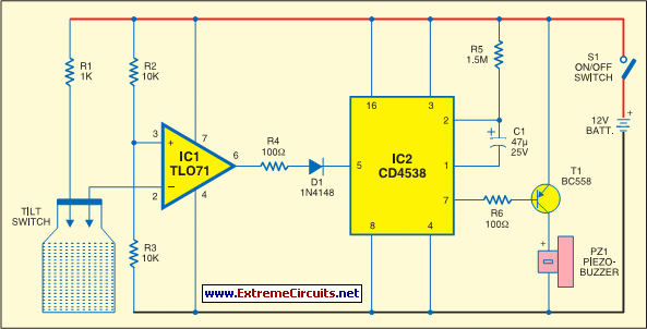
Protect your valuable laptop against theft using this miniature alarm generator. Fixed inside the laptop case, it will sound a loud alarm when someone tries to take the laptop. This highly sensitive circuit uses a homemade tilt switch to...
The power supply is standard. The 110VAC input connects to connector N17, in series with a power switch SW1, a fuse F1, and the primary coil of transformer T1. The secondary coil of T1 generates 24VAC at 12 Amps,...
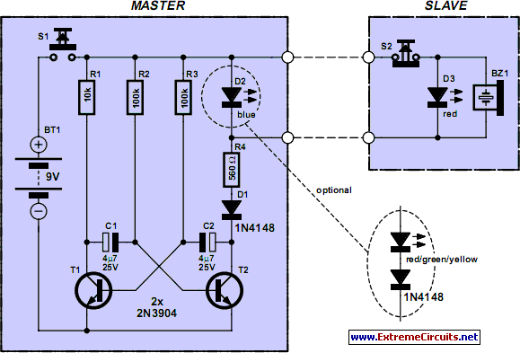
This circuit can be utilized by individuals, such as a gentleman summoning his butler, a manager calling for his secretary, or, as in the author's case, to call children down for dinner without raising one's voice over the noise...
The controller for a Hybrid Power Plant (HPP) block diagram consists of 440 Wp photovoltaic modules, a 1 kW wind turbine, and a 5 kW diesel engine as a backup. The HPP functions as a centralized PV and wind...

A small bias on the bases of Q1 and Q2 through R1 and R2 assists in initiating the circuit. This provides each transistor's base with a slight forward bias, enabling both transistors to conduct when the circuit is initially...
This chapter presents detailed schematics for various power supplies compatible with commonly available Ar/Kr ion tubes in the surplus market. It includes examples of commercial designs such as the Omnichrome 150R and 532 head, Lexel 88 and head, alongside...