
Multiplication circuit in broadband video band used

The circuit is designed to utilize differential inputs effectively, ensuring that the right amplifier's bias current exceeds the specified threshold of 800 nA. This characteristic is critical for maintaining the integrity of the input coupling capacitor, which plays a vital role in signal transmission. The resistance values applied to the input side, including the X2 balancing resistor, are essential for the circuit's operation as a balanced modulator.
The balanced modulator circuit is designed to suppress unwanted signals and enhance the desired modulated signal. The variable resistor, referred to as VRi, is integral to adjusting the input carrier modulated signal to zero, thus achieving equilibrium. This adjustment is crucial in preventing carrier leakage, which can lead to signal distortion and reduced performance.
Stability of the power supply circuit is paramount. Any instability can result in compromised load balancing, ultimately affecting the overall functionality of the circuit. The specified bandwidth of 10 MHz at -3 dB indicates the frequency range over which the circuit can operate effectively, allowing for signal processing within this limit.
When incorporating phase shift into the power circuit, attention must be given to the design to ensure that it does not introduce additional complications or degrade performance. The balance between phase shift and the desired output must be maintained to ensure optimal operation of the circuit. Proper implementation of these elements will lead to a robust and efficient design suitable for various applications in electronic systems.Although the respective inputs are differential inputs, but the right amplifier is greater than the general OP bias current (800nA), so as the input coupling capacitor, confide nce should be noted that the resistance value (on the input side should also be applied to the X2, balancing resistor, etc.) use it as a balanced modulator circuit assassination elbow, Yin from the input carrier modulated signal is equal to zero when adjusting variable resistor v roar to achieve equilibrium carriers (carrier leak happened). VRi power supply circuit using bad if the power supply stability, it will undermine the transition load balancing © Since bandwidth ioMHz/- 3d B.
Used in the phase shift of power when the road should be noted.
Related Circuits
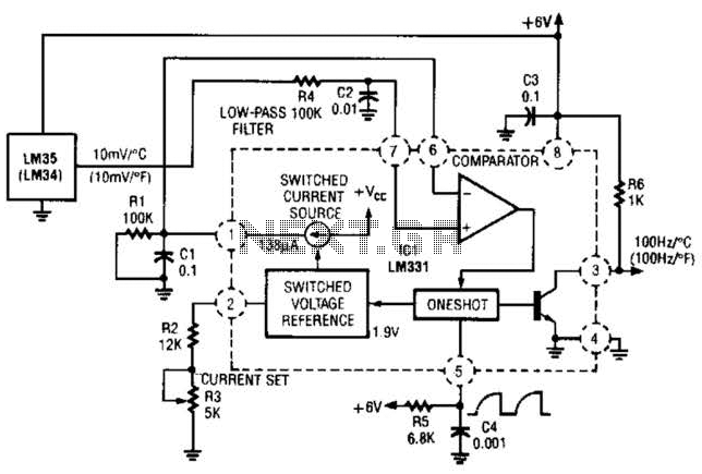
In this circuit, an LM34 or LM35 generates a frequency that is proportional to temperature. The reference current (138) is established through resistor R3. The output can be utilized to drive a display, frequency counter, or other indicating devices...

Transistors T1 and T2 form the microphone preamplifier. Resistor R1 provides the necessary bias for the microphone condenser, while preset VR1 functions as a gain control to adjust the gain level. To enhance audio power, the low-level audio output...
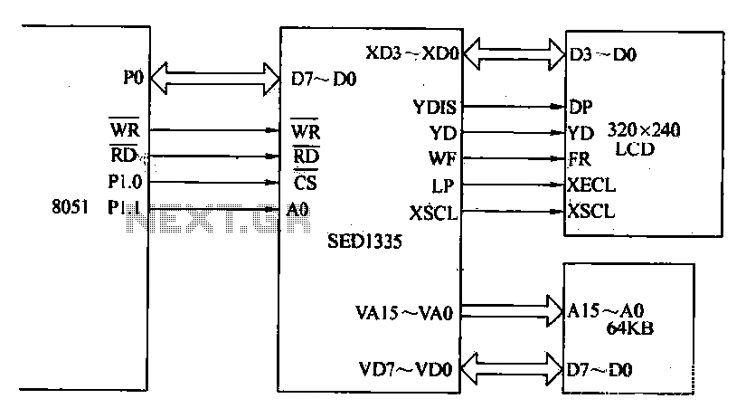
The MCS-51 series single-chip interface circuit 8051 is utilized to control the SED1335 35 dot matrix LCD display. This controller can manage up to a 640x256 dot matrix LCD display for both graphics and character representation, with the capability...

A stepper motor is a motor controlled by a series of electromagnetic coils. The center shaft has a series of magnets mounted on it, and the coils surrounding the shaft are alternately energized or de-energized, creating magnetic fields that...
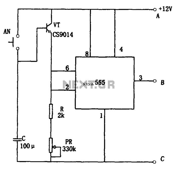
The circuit features a straightforward long timing mechanism. Activating switch AN initiates the timing process, while tone PR allows for timing adjustments. The timing range spans from 3 minutes to 220 minutes. With a capacitance value of 2200 µF,...
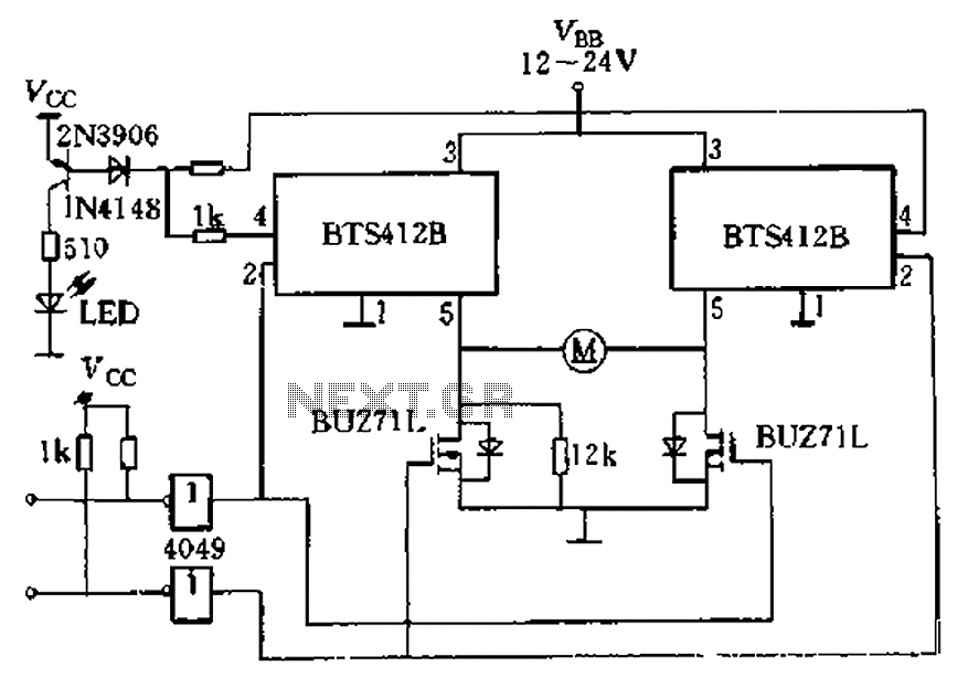
The BTS412B functions as two high-side power MOSFET switches, while two BU271L (50V, Zhang 1n) serve as low-side switches, forming a bi-directional H-bridge DC motor drive circuit. This configuration is designed for electrical automatic door systems, capable of handling...