
Negative Input Voltage Circuit using Voltage-to-Frequency Converter

The V/F converter circuit is essential in converting an analog voltage signal into a corresponding frequency output. The VFC32 is a specialized integrated circuit that performs this conversion with high precision and efficiency. In this configuration, the circuit is designed to accept negative input voltages, which is critical for applications that require signal processing of negative ranges.
The core operation of the VFC32 involves generating a frequency output that is directly proportional to the input voltage. The circuit typically includes components such as resistors, capacitors, and operational amplifiers that establish the necessary gain and filtering characteristics. In the case of negative input voltage, the circuit may incorporate level-shifting techniques to ensure that the input signal is correctly processed without distortion.
Key features of the VFC32 include a wide operating range, low temperature drift, and the ability to interface with digital systems, making it suitable for applications in instrumentation, control systems, and data acquisition. The output frequency can be measured using frequency counters or microcontroller-based systems, allowing for easy integration into larger electronic systems.
In summary, the V/F converter utilizing the VFC32 is a versatile and reliable solution for converting negative voltage inputs into frequency outputs, providing crucial functionality in various electronic applications.Here is the circuit diagram of V/F Converter in negative input voltage. It uses the VFC32 voltage-to-frequency converter. This VFC32 used to be applied in. 🔗 External reference
Related Circuits
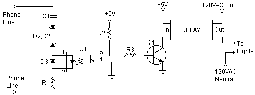
This document explains how to connect lights so that they flash when the phone rings. This setup is particularly beneficial in noisy environments, such as workshops, where it is challenging to hear the phone ringing. The ring detection component...
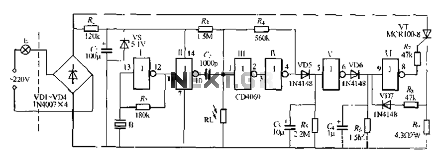
The circuit is designed for sound and light control of stairway and walkway lighting. It features high immunity and includes soft-start and over-current protection mechanisms. During the day, the photosensitive resistor has low resistance, resulting in a low voltage...
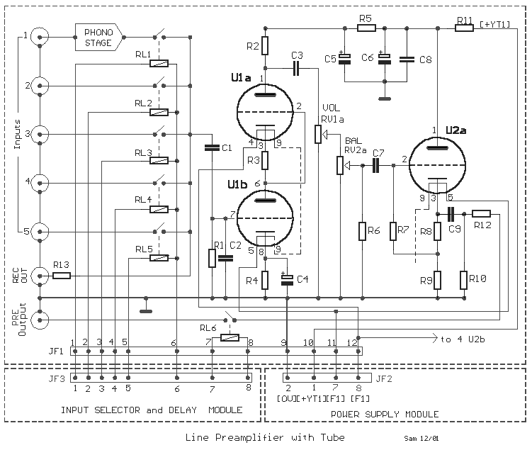
The circuit was designed to create a line preamplifier using double triode tubes. It consists of three parts, including the main preamplifier. The line preamplifier circuit utilizing double triode tubes is structured to enhance audio signals by amplifying low-level signals...
The circuit incorporates components Q, C, and ZD, which are responsible for the bias and buffer stages. Its primary objective is to ensure stable MOSFET gate operation and provide an offset voltage through a voltage buffer amplifier stage with...
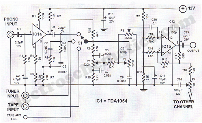
This Hi-Fi stereo preamplifier circuit is designed using the TDA1054 integrated circuit from SGS. The TDA1054 is a 16-pin DIL package that incorporates two separate preamplifier circuits. It is a low-noise preamplifier with minimal complications in the design process....

This simple circuit indicates the status of a phone, including Line OK, Dialing, and Call Attended. It also features a locking mechanism to block outgoing calls while allowing incoming calls, preventing misuse of the telephone. The circuit requires only...