
NFC Tag communication system

The circuit design involves calculating the resonance capacity using a specific formula, which is essential for optimizing the performance of the NFC (Near Field Communication) system. The NFC Tag LSI, or Large Scale Integration, is a critical component that facilitates communication between the NFC tag and the reader.
The antenna circuit board is designed to support the NFC Tag LSI, ensuring that it can effectively transmit and receive signals. The resonance frequency of the antenna is a crucial parameter that affects the efficiency of the NFC communication. This frequency must be precisely measured to ensure that the antenna operates at its optimal performance level.
After measuring the resonance frequency, adjustments to the resonance capacity are necessary. This adjustment process may involve changing the values of capacitors in the circuit or altering the physical dimensions of the antenna to achieve the desired resonance frequency.
The overall goal of this process is to ensure that the NFC system operates reliably and efficiently, facilitating seamless communication in applications such as mobile payments, access control, and data transfer. Proper tuning of the resonance capacity directly impacts the range and effectiveness of the NFC communication, making it a vital aspect of the circuit design.A calculating resonance capacity from formula (1) and NFC Tag LSI are set to antenna circuit board, and measured resonance frequency, after that, adjusting resonance capacity 🔗 External reference
Related Circuits
In the precision circuit, an operational amplifier provides a buffered output and also functions as a 2-pole filter. The ripple will be less than 5 mV peak for all frequencies above 1 kHz, and the response time will be...
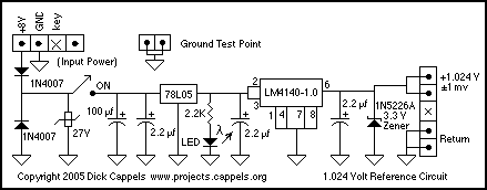
A keyed power input connector, series rectifier and a shunt rectifier, both 1N4007, prevent reverse voltage from being applied to the power input. A 27 volt metal oxide varistor clamps the voltage to the 78L05 that follow it, to...
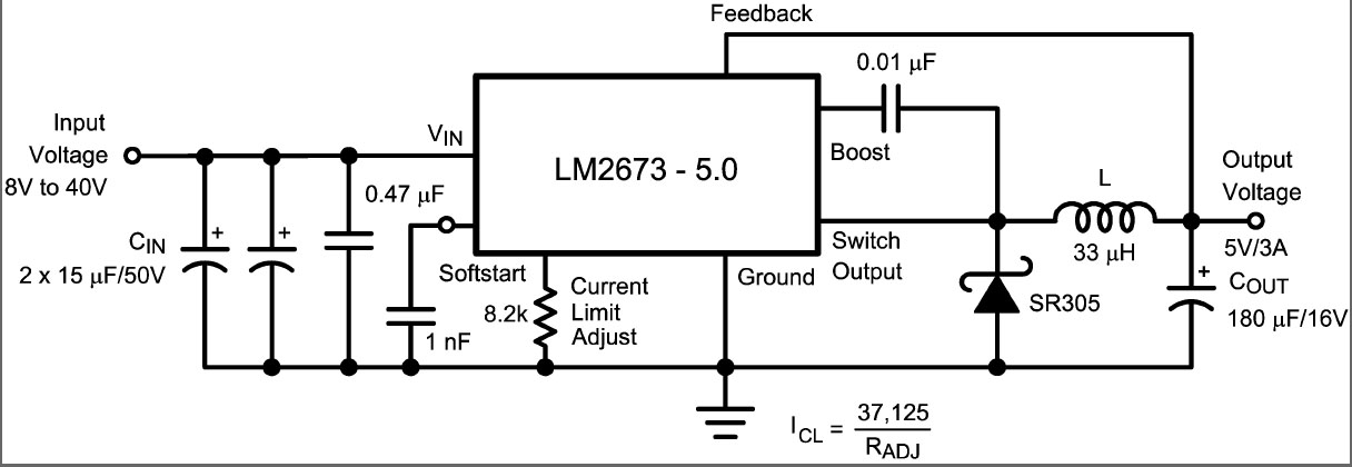
This is a DC switching regulator with an output voltage of 5V and a maximum current of 3A. It is designed for use in digital circuits. The key component of the circuit is the LM2673, which is a 3A...

The AD7740 is the smallest and most affordable 12-bit Voltage-to-Frequency Converter (VFC) available. As a synchronous converter, its output frequency is tied to a fixed master clock frequency, which enhances temperature stability compared to asynchronous VFCs. With a 1...
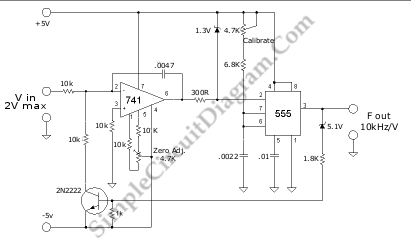
A voltage-to-frequency converter (VFC) circuit is illustrated in the schematic diagram below. The circuit utilizes a 555 integrated circuit (IC) as the central component of its operation. The voltage-to-frequency converter (VFC) is a crucial electronic circuit that converts an input...
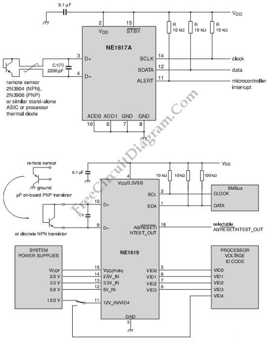
This is a circuit of a board system monitoring the temperature and voltage conditions. It uses the NE1617A, which is a 2-channel temperature sensor. The described circuit serves as a monitoring system for both temperature and voltage conditions, utilizing the...