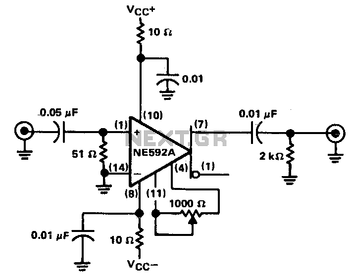
Oscilloscope-counter-preamplifier

The circuit provides a voltage gain of 20 ±0.1 dB within a frequency range of 500 kHz to 50 MHz. The low-frequency response of the amplifier can be enhanced by increasing the value of the 0.05 µF capacitor connected in series with the input terminal. The circuit achieves an input noise level of approximately 10 µV across a bandwidth of 15.7 MHz. Additionally, the gain can be calibrated by adjusting the potentiometer connected between pins 4 and 11. A 1 kΩ potentiometer can be fine-tuned to achieve an exact voltage gain of 10, thereby maintaining the scale factor of the instrument.
The described circuit is a wideband amplifier designed to deliver a consistent voltage gain across a specified frequency range. The gain of 20 ±0.1 dB indicates a relatively high amplification suitable for various applications, including signal conditioning and instrumentation. The frequency range of 500 kHz to 50 MHz suggests that this amplifier is suitable for RF applications, where maintaining signal integrity is crucial.
To enhance the low-frequency response, the circuit incorporates a 0.05 µF capacitor in series with the input terminal. Increasing the capacitance value will lower the cutoff frequency, allowing the amplifier to respond effectively to lower frequency signals. This adjustment is particularly useful in applications where low-frequency signals are of interest.
The input noise level of approximately 10 µV is indicative of the circuit's performance in minimizing noise, which is essential for accurate signal processing. The specified bandwidth of 15.7 MHz implies that the circuit is designed to handle signals within this range effectively, ensuring that the amplifier does not introduce significant distortion or noise.
The inclusion of a potentiometer between pins 4 and 11 allows for precise calibration of the gain. The use of a 1 kΩ potentiometer provides flexibility in adjusting the gain to achieve an exact value of 10. This feature is crucial in applications where precise gain settings are necessary to maintain the accuracy and reliability of measurements. By preserving the scale factor of the instrument, the circuit ensures that the output remains proportional to the input, facilitating accurate data interpretation.
Overall, the circuit's design emphasizes versatility and precision, making it suitable for a range of electronic applications where signal amplification is required.The circuit will provide a 20 ±0.1 dB voltage gain from 500 kHz to 50 MHz. The low-frequency response of the amplifier can be extended by increasing the value of the 0.05-JLF capacitor connected in series with the input terminal. This circuit will yield an input-noise level of approximately 10 !LV over a 15.7-MHz bandwidth. The gain can be calibrated by adjusting the potentiometer connected between pins 4 and 11. The 1-KO potentiometer can be adjusted for an exact voltage gain of 10. This preserves the scale factor of the instrument.