
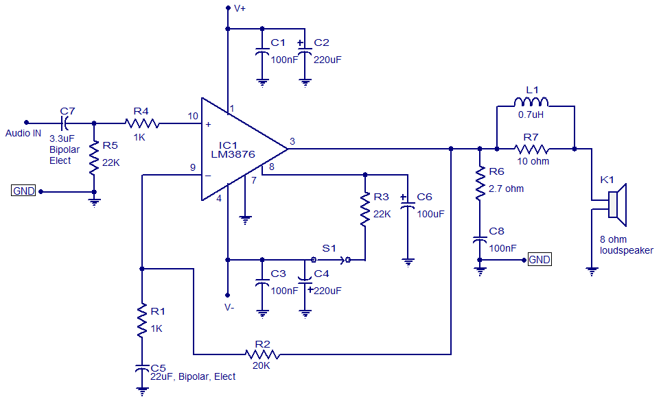
The LM3886 BTL amplifier

The LM3886 amplifier circuit is designed to provide high-fidelity audio amplification, making it suitable for various audio applications. The NE5532 preamplifier serves to enhance the input signal before it is processed by the LM3886 power amplifier, which is known for its low distortion and high output capability. The power supply requirements are critical; a transformer with a capacity of 300 to 400 VA is recommended to ensure that the amplifier can deliver its maximum output without clipping or distortion. The dual secondary windings of 28 V each allow for sufficient voltage to drive the amplifier effectively.
The rectifier bridge, rated at 15 A, must be capable of handling the current demands of the amplifier during peak output conditions. The filter capacitor should be of high capacitance to smooth out the rectified voltage and provide stable power to the amplifier, which is crucial for maintaining audio quality. It is advisable to select high-quality capacitors with low equivalent series resistance (ESR) to minimize power loss and improve transient response.
Thermal management is a significant consideration in the design of the LM3886 amplifier. The heat sink must be appropriately sized to dissipate the heat generated during operation, ensuring that the amplifier remains within safe operating temperatures. The use of thermal grease between the amplifier chip and the heat sink should be minimized to reduce thermal resistance, which can hinder effective heat dissipation.
Moreover, the layout of the printed circuit board (PCB) is crucial for the performance of the amplifier. Proper isolation between the input and output circuits is necessary to prevent feedback and interference that could degrade audio quality. The design should also incorporate short signal paths to minimize inductance and capacitance, which can lead to unwanted noise and self-excitation. An input capacitor can be employed to filter out high-frequency noise, ensuring that only the desired audio frequencies are amplified.
This comprehensive approach to the design and implementation of the LM3886 amplifier circuit will facilitate the achievement of high-quality audio output while ensuring reliability and performance.Figure 2-60 is LM3886 amplifier roar practical circuit, the circuit with one NE5532 as preamplifier, output power up to 200Wo. LM3886 power amplifier for use, due to the large output power, must have adequate power supply in order to obtain high-quality output. When the two-channel, power transformer capacity should be 300 ~ 400 f ~, dual secondary windings each 28Vo rectifier bridge should 15A, crossing the filter capacitor only to large capacity, and should be of good quality. Since the output power, equipped with a heat sink should have sufficient cooling area, and reduce the use of thermal grease resistance o-made printed circuit board should pay attention to the input and output isolation of the circuit.
Signal input line should be short, to prevent self-excited, input capacitance C can eliminate high-frequency self-excited.
Related Circuits
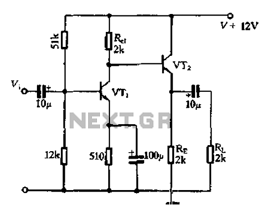
Available RC coupling between its two stages can also be directly coupled. This is in addition to the common-emitter total radio circuit configuration, which is widely used. Outside the previously described common-emitter circuit, a total group or common-emitter circuit...
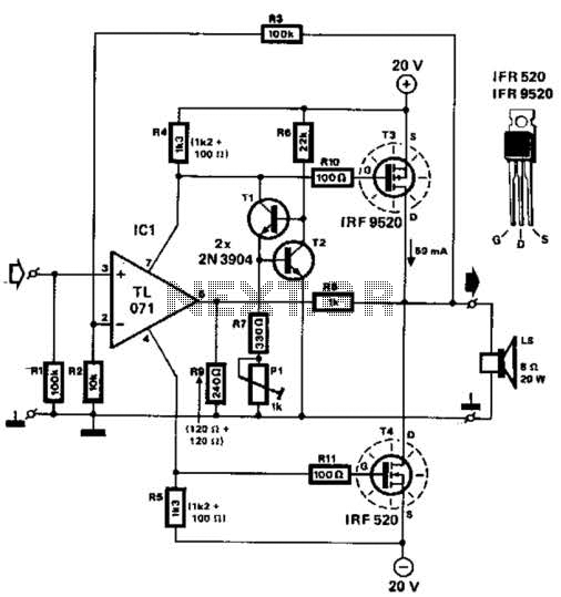
Two complementary MOSFETs are utilized to deliver 20 W into an 8-ohm load. A TL071 operational amplifier serves as the input amplifier. The MOSFETs must be equipped with a heatsink that has a thermal resistance of better than 5...
LM3876-based 50-watt audio amplifier circuit. Operates from +/-35V DC. Simple design, low noise. The LM3876 is a high-performance audio power amplifier designed for driving speakers in various audio applications. This particular circuit configuration enables the amplifier to deliver up to...

A microphone preamplifier utilizing a CMOS operational amplifier powered by its own battery is compact enough to fit within a small microphone casing. The amplifier functions with a 1.5V battery and exhibits low supply currents. This preamplifier operates at...
This circuit is not easy to build, but it provides excellent audio quality. It serves as a high-quality preamplifier, capable of driving high-quality power amplifiers while delivering good sound. The described circuit functions as a high-fidelity audio preamplifier, designed to...
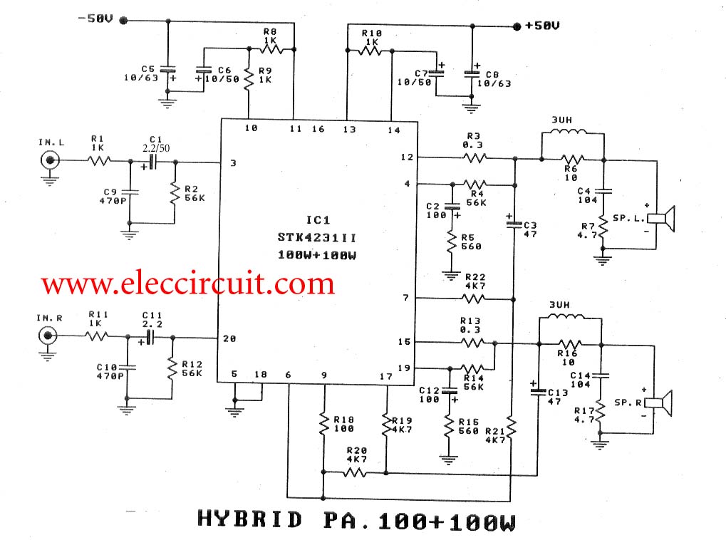
To create a 100-watt OCL audio amplifier circuit, consider using this design. It incorporates the STK4231 integrated circuit, which is a compact and cost-effective solution. The STK4231 is a hybrid IC from Sanyo, belonging to the STK4201II series, capable...