
Positive-input-negative-output-charge-pump
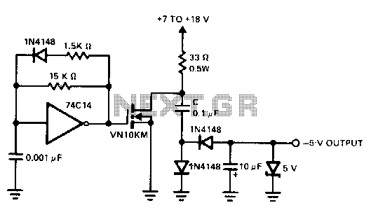
A charge pump is a straightforward method for generating a low-power voltage supply of opposite polarity from the main supply. The 74CL4 IC serves as a self-oscillating driver for the MOSFET power switch, producing a pulse width of 6.5 microseconds at a repetition frequency of 100 kHz. When the MOSFET device is off, capacitor C is charged to the positive supply. When the power through the MOSFET is switched on, capacitor C delivers a negative voltage through the series diode to the output. The zener diode functions as a dissipative regulator. Due to the rapid switching of the MOSFET, operation at high frequencies enables the use of smaller capacitors in the system.
A charge pump circuit is designed to convert a DC voltage from a primary source into a negative voltage supply, which is particularly useful in applications requiring dual polarity supplies, such as operational amplifiers and analog signal processing. The core component of this circuit is the 74CL4 integrated circuit, which is an essential self-oscillating driver. This IC generates a square wave signal with a pulse width of 6.5 microseconds at a frequency of 100 kHz, which is ideal for efficiently driving the MOSFET switch.
In the circuit operation, when the MOSFET is in the OFF state, the capacitor C is charged to the positive supply voltage, effectively storing energy. Upon switching the MOSFET ON, this stored energy is released, and capacitor C discharges, resulting in the generation of a negative output voltage. The series diode is critical in this process, as it allows the negative voltage to be directed to the output while preventing backflow of current to the capacitor.
The inclusion of a zener diode in the circuit acts as a dissipative regulator, maintaining the output voltage at a stable level by clamping it to a predetermined value. This regulation is crucial for protecting downstream components from voltage spikes and ensuring consistent performance.
The high-frequency operation of the MOSFET allows for the use of smaller capacitors within the circuit, which is advantageous for reducing the overall size and cost of the electronic design. Smaller capacitors can also lead to lower equivalent series resistance (ESR), enhancing the efficiency of the charge pump. Overall, this charge pump design is efficient, compact, and suitable for a variety of low-power applications requiring negative voltage supplies.A charge pump is a simple means of generating a low-power voltage supply of opposite polarity from the main supply. The 74Cl4 IC is a self-oscillating driver for the MOSFET power switch. It produces a pulse width of 6.5 p,s at a repetition frequency of 100 kHz. When the MOSFET device is off, capacitor C is charged to the positive supply. When the power through the MOSFET switches on, C delivers a negative voltage through the series diode to the output.
The zener serves as a dissipative regulator. Because the MOSFET switches fast, operation at high frequencies allows the capacitors in the system to be small. 🔗 External reference