
Rf-modulator
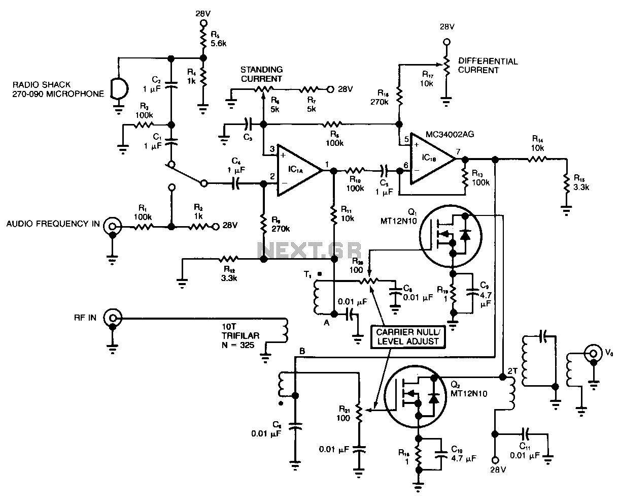
Power MOSFETs provide high power gain at both audio and radio frequencies, making them valuable in various radio circuit designs. For RF applications, the large safe operating area of a MOSFET protects it from damage caused by reflected RF energy. As a modulator, the transfer linearity of a MOSFET enhances fidelity. In a suppressed-carrier modulator, an RF signal is applied to the primary of transformer T1, whose secondaries deliver equal-amplitude, opposite-phase RF drive signals to output FETs Q1 and Q2. The output voltage (Vout) is zero when no audio-frequency signals are present, as the opposite-phase RF signals from Q1 and Q2 cancel each other out. When audio-frequency signals are introduced at nodes A and B, a modulated RF output is produced. Source resistors R18 and R19 enhance the DC stability and low-frequency gain. A phase inverter, utilizing the dual op-amp IC1A and IC1B, generates the out-of-phase, equal-amplitude audio-frequency modulation signals.
Power MOSFETs are integral components in RF circuit designs due to their ability to handle high power levels while maintaining linearity across a wide frequency range. The device's large safe operating area is critical in RF applications, as it allows the MOSFET to withstand voltage and current spikes that can occur from reflected RF energy, thereby preventing potential damage.
In the context of a suppressed-carrier modulator, the RF signal input is coupled into the primary winding of transformer T1. The transformer is designed to produce two secondary outputs that are equal in amplitude but 180 degrees out of phase. This configuration is essential for driving the output FETs Q1 and Q2, which are responsible for generating the modulated RF output.
When no audio signals are present, the voltages at the outputs of Q1 and Q2 are equal and opposite, resulting in a net output voltage (Vout) of zero. The introduction of audio-frequency signals at nodes A and B disrupts this balance, allowing the modulation of the RF output, which can be observed as variations in Vout corresponding to the audio input.
To enhance the performance of the circuit, source resistors R18 and R19 are employed. These resistors play a significant role in stabilizing the DC operating point of the circuit while also improving the low-frequency gain, which is crucial for audio applications.
The phase inverter circuit, constructed using the dual op-amp IC1A and IC1B, is responsible for generating the necessary out-of-phase modulation signals. By utilizing the characteristics of the op-amps, the circuit ensures that the modulation signals are of equal amplitude, which is vital for maintaining the integrity of the modulation process and achieving high fidelity in the output signal.
Overall, this configuration exemplifies the effective use of MOSFETs in RF modulation applications, leveraging their inherent properties to create reliable and efficient circuit designs.Because power MOSFETs offer high power gain at both audio and radio frequencies, they are useful in many areas of radio-circuit design. For rf applications, a MOSFET"s large safe operating area, V0 s vs ! 0, protects it against damage from reflected rf energy. As a modulator, a MOSFET"s transfer linearity aids fidelity. In the suppressed-carrier modulator, an rf signal is applied to the primary of transformer Tl, whose secondaries provide equal-amplitude, opposite-phase rf drive signals to output FETs Ql and Q2.
Output V. is zero when no audio-frequency signals are present, because the opposite-phase rf signals from Ql and Q2 cancel. When audio-frequency signals appear at nodes A and B, you obtain a modulated rf output (I";,). Source resistors Rl8 and Rl9 improve the de stability and low-frequency gain. A phase inverter, based on the dual op amp IClA and IClB, generates the out-of-phase, equal-amplitude, audio-frequency modulation signals.
🔗 External reference
Related Circuits
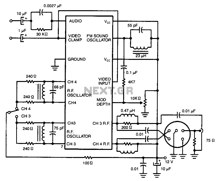
Two integrated circuit (IC) RF modulators convert a suitable baseband video and audio signal to a low VHF modulated carrier, specifically Channel 2 through 6 in the U.S. and Channels 1 through 3 in Japan. The LM1889 and LM2889...