
RF2103P schematic configuration of 915MHz RF amplifier

The RF2103P is a high-performance RF amplifier designed for operation at 915MHz, commonly used in various wireless communication applications. The circuit configuration includes several key components that facilitate its operation.
P1, the power connector, is essential for providing the necessary voltage and ground reference to the amplifier. The Vcc connection (P1-1) supplies the required power for the amplifier's operation, while the ground connection (P1-2) ensures stable reference levels for signal processing. The power down control (P1-3) allows for the amplifier to be turned off when not in use, thereby conserving power.
The RF input socket (J1) is where the input signal is fed into the amplifier. This input stage is crucial as it determines the overall performance characteristics, including gain and linearity. The RF output socket (J2) provides the amplified signal to the subsequent stages of the system or to the antenna, depending on the application.
In addition to these primary components, proper impedance matching is vital for maximizing power transfer and minimizing signal reflections at both the input and output stages. This may involve the use of additional passive components such as resistors, capacitors, and inductors to create matching networks tailored to the specific requirements of the 915MHz frequency.
Thermal management is also an important consideration in the design of the RF2103P amplifier circuit. Adequate heat dissipation mechanisms, such as heat sinks or thermal vias, should be implemented to ensure that the amplifier operates within its specified temperature range, thus maintaining reliability and performance.
Overall, the RF2103P 915MHz RF amplifier circuit is a sophisticated design that requires careful consideration of power supply, input/output configurations, impedance matching, and thermal management to achieve optimal performance in wireless communication systems. As shown in FIG constituted by RF2103P 915MHz RF amplifier circuit. P1 for the outlet, which P1-1 take power Vcc, P1-2 ground, P1-3 then power down control voltage VB; J1 to th e RF input socket; J2 as RF output socket.
Related Circuits
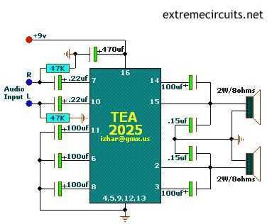
The above circuits are based on TEA2025, a monolithic integrated audio amplifier in a 16-pin plastic dual in-line package manufactured by UTC. The circuit has an internal thermal protector and is designed for portable cassette players and radios. It...
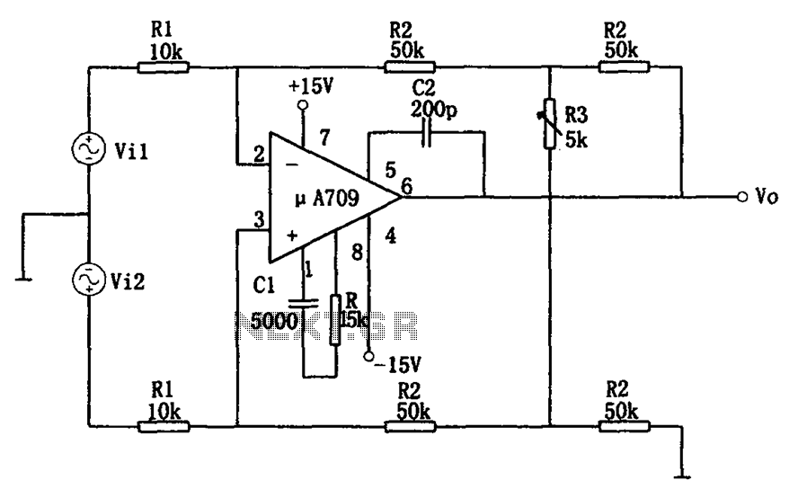
The configuration of the variable gain A709 differential amplifier circuit is illustrated. The primary advantage of this circuit is its ability to maintain a constant common-mode rejection ratio (CMRR) while allowing for continuous adjustments to the differential gain. The...

Part of the challenge is that multiple capacitors and resistors are present in the RIAA circuit. This is derived from the Harman-Kardon schematic. The information for the Citation IV is not readily available, but it is simpler to replace...
A TSOP4156 is often difficult to obtain or expensive to purchase. In response, an individual utilized old BPW41 infrared diodes to construct a custom receiver. The power source is derived from the RS232 port, requiring a minimum of 5.5...
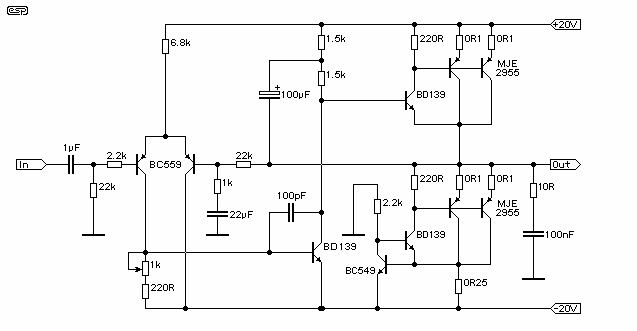
This amp uses the basic circuitry of the 60W power amp but modified for true Class-A operation. This amp has been built by several readers, and the reports I have received have been very positive. With simulations, everything appears...
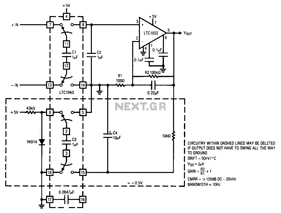
This circuit operates from a single 5 V power supply. The LTC1043 switched-capacitor instrumentation building block facilitates a differential-to-single-ended transition using a flying-capacitor technique. The circuit alternately samples the differential input signal and charges the ground-referred capacitor C2 with...