Sawtooth-and-pulse-generator

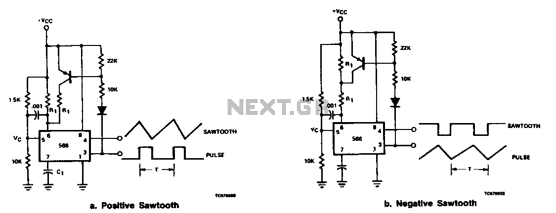
The output at pin 3 of the 566 can be utilized to deliver varying charge and discharge currents for capacitor Cl, resulting in a sawtooth waveform available at pin 4 and a pulse output at pin 3. It is essential for the PNP transistor to be adequately saturated to maintain optimal temperature stability. The charge and discharge durations can be approximated using the provided formula, where Rr represents the total resistance between pin 6 and Ycc for the specified interval.
The 566 integrated circuit functions as a voltage-controlled oscillator (VCO) and is widely used in applications requiring precise timing and waveform generation. In this configuration, the output from pin 3 serves as a pulse generator, while pin 4 produces a sawtooth waveform. The sawtooth waveform is particularly useful in applications such as signal modulation and waveform shaping.
To achieve the desired output characteristics, the PNP transistor connected to pin 3 must be driven into saturation. This ensures that the transistor operates in a region where it can effectively switch between its on and off states with minimal voltage drop, thereby enhancing temperature stability and performance. The saturation of the transistor is crucial because variations in temperature can affect the charge and discharge rates of the capacitor, leading to inaccuracies in the generated waveforms.
The charge and discharge times of capacitor Cl can be calculated using the formula provided, which takes into account the combined resistance Rr between pin 6 and the supply voltage Ycc. The resistance influences the time constants associated with charging and discharging the capacitor, directly affecting the frequency and duty cycle of the output waveform. By adjusting Rr, one can fine-tune the output frequency and ensure that the waveform meets the requirements of the specific application.
In summary, the configuration of the 566 IC with a well-saturated PNP transistor and appropriately chosen resistances allows for the generation of precise waveforms, making it suitable for various electronic applications requiring timing and signal processing.The pin 3 output of the 566 can be used to provide different charge and discharge currents for Cl so that a sawtooth output is available at pin 4 and a pulse at pin 3. The pnp transistor should be well saturated to preserve good temperature stability. The charge and discharge times can be estimated by using the formula shown. Where Rr is the combined resistance between pin 6 and Ycc for the interval considered.