Self-oscillating-switching-converter

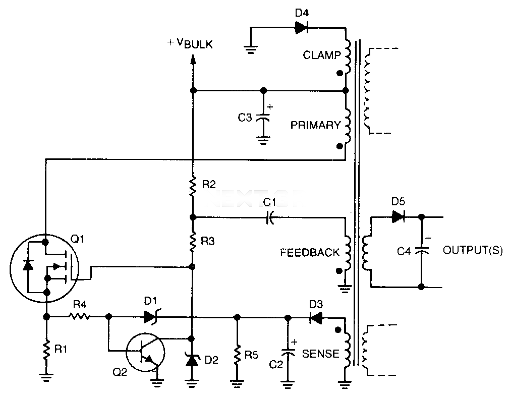
Regulation is achieved by using the rectified output from the sense winding, which is applied as a bias to the base of transistor Q2 through Zener diode D1. The collector of Q2 then disconnects the drive from the gate of transistor Q1. Consequently, if the output voltage increases, Q2 reduces the drive to Q1 sooner, thereby shortening the on-time and maintaining a constant output voltage. The outputs are obtained by rectifying and filtering the secondary windings, as demonstrated by diode D5 and capacitor C4.
In this circuit, the regulation mechanism relies on feedback from the output voltage to control the operation of the transistors. The sense winding monitors the output voltage, and its rectified signal serves as a reference for the biasing of Q2. Zener diode D1 plays a critical role in stabilizing the voltage applied to the base of Q2, ensuring that it operates within a defined range. When the output voltage rises above a predetermined level, the increased bias at the base of Q2 causes it to conduct more, which in turn lowers the gate drive to Q1. This action effectively reduces the conduction time of Q1, preventing the output voltage from exceeding the desired level.
The rectification and filtering of the secondary windings are essential for providing a stable DC output. Diode D5 is responsible for converting the AC voltage from the secondary winding into a pulsating DC voltage, while capacitor C4 smooths this output, reducing ripple and providing a more stable voltage to the load. The combination of these components ensures that the circuit can maintain a consistent output voltage despite variations in load or input voltage, making it suitable for applications requiring precise voltage regulation.Regulation is provided by taking the rectified output of the sense winding and applying it as a bias to the base of Q2 via zener Dl. The collector of Q2 then removes drive from the gate of Ql. Therefore, if the . output voltage should increase, Q2 removes the drive to Ql earlier, shortening the on time, and the output voltage will remain the same.
De outputs are obtained by merely rectifying and filtering secondary windings, as done by D5 and C4.