
simple bus level-shift / I2C mosfet level converter Fairchild BSS138

The circuit described utilizes a method for voltage level shifting in I2C bus applications, particularly beneficial when interfacing components with different operating voltages. The BSS138 MOSFETs serve as level shifters, effectively translating the 3V logic levels of the ATMEL AT90S8515 microcontroller to the 5V requirements of the Seiko LCD module. This arrangement is crucial for maintaining compatibility between devices that operate at different voltage levels, ensuring reliable data communication.
In the schematic, the pull-up resistors connected to the drain of each MOSFET play a vital role in defining the logic levels on the I2C bus. The choice of resistor values can influence the rise time of the signals and overall bus performance. The three tested resistor values—100k, 10k, and 4.7k ohms—demonstrate that the circuit remains functional across a range of pull-up configurations. The lower the resistance value, the faster the signal rise time, which can be advantageous in high-speed communication scenarios.
The design also incorporates the ability to isolate sections of the I2C bus by pulling the gates of the MOSFETs low. This feature is particularly useful for debugging or when multiple devices are connected to the bus, allowing for selective communication and reducing potential conflicts.
Overall, the implementation of this circuit provides a robust solution for interfacing devices with differing voltage levels on the I2C bus, while maintaining simplicity and effectiveness in design. The application note by Mr. Schutte serves as a valuable resource for engineers looking to explore advanced I2C bus interfacing techniques.While doing some background reading about the Philips I2C bus I came across an application note written by Herman Schutte (of Philips Semiconductors Systems Laboratory in Eindhoven). Mr. Schutte described an elegant mechanism for interfacing sections of I2C-bus which are operating at different voltages through the use of MOSFETs and pull-up resist
ors. I had also been looking at a number of options for interfacing a 5V LCD panel to a microcontroller system that I wanted to run at 3V and so decided to try applying this idea to the data and control lines in my circuit. Although I was building the circuit by hand I decided to use a surface mount package for the MOSFETs.
As three-terminal devices they are relatively easy to solder as long as you can hang onto them. The image above on the right shows some of the 11 MOSFETs in use on the 0. 1" proto board. I used the Fairchild Semiconductor BSS138 (datasheet) N-channel enhancement mode MOSFET which is available in the standard SOT-23 package from folks like Digi-Key. Below on the right are wave forms for the circuit using three different values for the pull-up resistors: 100k, 10k and 4.
7k ohms. These values were picked from what I had close at hand. The circuit functions with any of them in fact. A basic drawing for the circuit I`m using is here. (or here for browsers without JavaScript. ) As the schematic shows, the circuit is remarkably simple and straight-forward. I have this circuit in-use with an ATMEL AT90S8515 (at 3. 6864Mhz) controlling a Seiko L203400J000 20x4 character LCD module. The 8515 is connected to a 3V supply while the LCD requires 5V. The control lines, RS, RW and E and the data lines D0-D7 are each level-shifted with the BSS138 MOSFETs. The level-shifting imposes no directionality on the bus so both reading from and writing to the LCD are possible.
An interesting feature of the circuit is that two halfs of the bus can be isolated from each other by pulling the FET gates low. Mr. Schutte describes a number of similar extensions to his basic circuit idea and discusses the necessary MOSFET features as well as some results.
The original (pre-NXP) link for AN97055 was: AN97055 and searchable at the Philips Semiconductor site under the I2C support area (enter the Application Note name AN97055): here. 🔗 External reference
Related Circuits
Precious metals can sometimes be buried too deep to be detected without complex devices. However, smaller pieces of precious metals located near the surface can often be found using simpler methods. Many individuals are drawn to the prospect of...
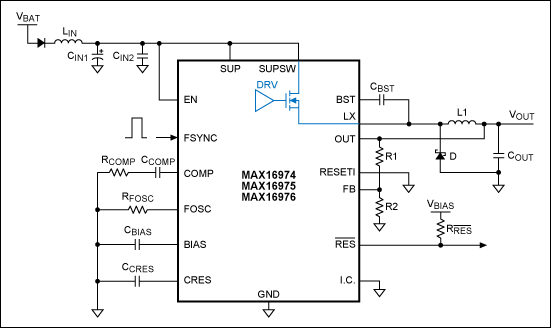
Cost, size, resistance, and current capability drive the choice of inductor for most step-down DC-DC switching converters. Inductors play a crucial role in the operation of step-down DC-DC switching converters, influencing performance parameters such as efficiency, output voltage stability, and...
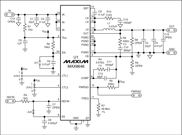
Optimize the layout of the MAX16974/MAX16975/MAX16976 high-performance DC-DC converters, which are standard buck controllers designed for automotive applications. The MAX16974, MAX16975, and MAX16976 are advanced DC-DC buck converters specifically tailored for automotive environments. These devices are engineered to deliver high...
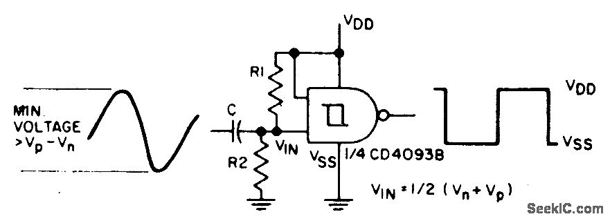
The sine input is AC coupled by capacitor C. Resistors R1 and R2 bias the input midway between Vn and Vp, the input threshold voltages, to provide a square wave at the output. The circuit described utilizes an AC coupling...
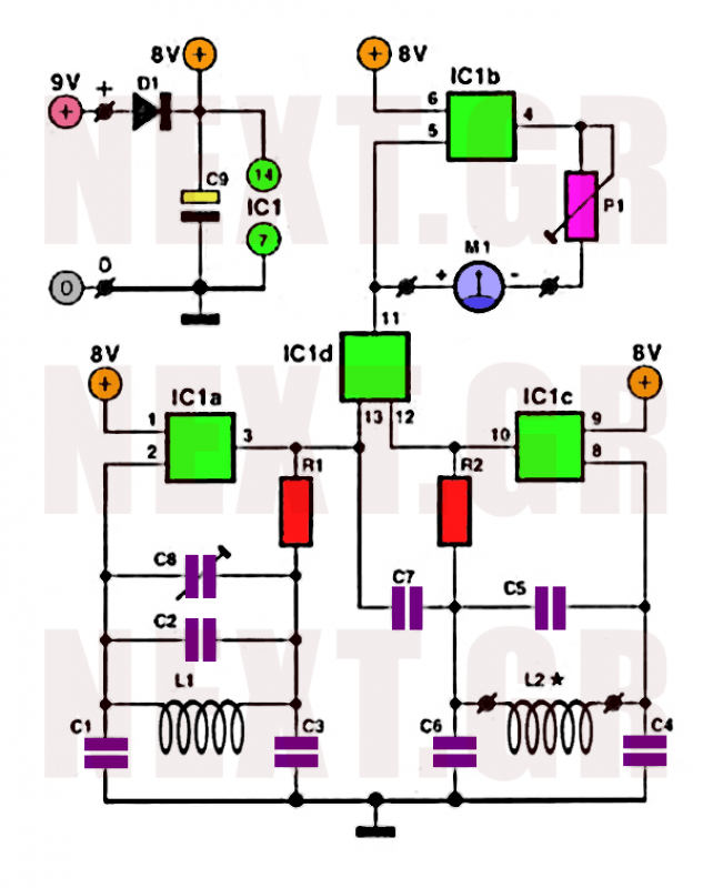
The FM broadcast band was relocated immediately after World War II from its original frequency just below 50 MHz to the current 88-108 MHz range. Hallicrafters was one of the companies that provided receiving converters for users of older...

This is a crystal radio circuit that features a simple design but is ineffective in tuning to the medium wave AM broadcast band. Component: Antenna. The crystal radio circuit operates on the principle of radio wave detection using a crystal...