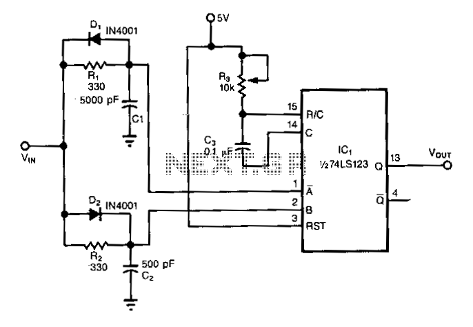
Single-chip-frequency-doubler

The frequency doubler utilizes a single integrated circuit (IC). Similar to other frequency doublers, this circuit leverages both the rising and falling edges of the input signals to generate digital pulses, effectively doubling the input frequency. In the absence of the RC networks at the inputs of IC1, no output pulses would be produced. The RC networks introduce a delay between the edges of the signals; specifically, the A input lags the B input for positive-going edges, while the B input lags the A input for negative-going edges. Additionally, the output duty cycle can be adjusted from 0% to 100% by varying resistor R3. The minimum output pulse width of IC1 determines the maximum frequency of this circuit.
The frequency doubler circuit is designed to enhance signal processing capabilities in various electronic applications. The core component, IC1, is typically a digital logic IC capable of handling high-frequency signals. The configuration of the circuit allows for the generation of pulses at twice the frequency of the input signal by utilizing the edges of the waveform. The RC networks play a crucial role in this process by introducing phase shifts between the input signals, thereby enabling the circuit to capture both the rising and falling edges effectively.
The resistor R3 serves as a variable component that influences the duty cycle of the output signal. By adjusting R3, the charge and discharge times of the capacitors in the RC networks can be modified, which in turn affects the width of the output pulses. This feature is particularly useful in applications where specific timing characteristics are required, such as in pulse width modulation (PWM) systems.
The maximum frequency capability of the frequency doubler is inherently linked to the minimum pulse width generated by IC1. As the frequency increases, the pulse width must remain within the operational limits of the IC to ensure reliable output. Therefore, careful selection of components, including the values of the resistors and capacitors in the RC networks, is essential to optimize the performance of the circuit.
In summary, this frequency doubler circuit exemplifies a straightforward yet effective approach to frequency manipulation, suitable for a variety of applications in communication and signal processing. By utilizing a single IC and adjustable components, it provides flexibility and ease of integration into larger systems.The frequency doubler uses only one !C. Like other doublers, this circuit uses both the rising and falling edges of the input signals to produce digital pulses, thus effectively doubling the input"s frequency. Without the rc networks at IC1 inputs, IC1 would not produce any output pulses. However, the rc networks delay one edge with respect to the other. The A input lags the B input for positive-going edges, and the B input lags the A input for negative-going ones.
You can vary the output duty cycle from 0 to 100% by varying R3. IC1"s minimum output pulse width defines the maximum frequency of this circuit.