
Single to double power with CA3140

The described circuit is a voltage divider configuration that is enhanced with buffer amplification to ensure stable output current delivery. The circuit utilizes a combination of resistors, capacitors, and transistors to achieve its functionality.
The resistors R1 and R3 are configured to set the voltage division ratio. R1 has a resistance of 22k ohms, and R3 has a resistance of 150k ohms. The output voltage is influenced by the values of these resistors, which can be calculated using the voltage divider formula. R4, valued at 1.5k ohms, likely serves a role in biasing or as part of a feedback loop.
Capacitors C1 and C2, both rated at 10uF and 35V, are used for filtering and stabilization of the voltage output, ensuring that any fluctuations are smoothed out. Capacitors C3 and C4, rated at 100nF, are likely used for high-frequency bypassing, providing stability in the presence of transient signals.
Transistor T1, a 2N3904, is a general-purpose NPN transistor used for switching or amplification purposes. T2 (TIP127) and T3 (TIP122) are power transistors that can handle higher currents, with T2 being a PNP Darlington pair and T3 being an NPN Darlington pair. These transistors act as buffers, allowing the circuit to deliver a current between 200 to 300 mA, which is crucial for driving loads that require more current than the voltage divider alone can provide.
The operational amplifier CA3140 is included in the circuit, likely serving as an active component for further signal processing or feedback control. Its role may involve amplifying the output signal or providing additional gain to ensure that the desired output voltage level is maintained.
Overall, this circuit design effectively combines passive and active components to create a robust voltage regulation solution suitable for applications requiring a stable output from a single voltage source.Another circuit for a balanced diet from a single voltage network. In fact, this is a uitbreding the other voltage divider circuit using a some power darling tons as buffer. This buffer can deliver a 200 to 300 mA. R1, R1 = 22k R3 = 150k R4 = 1.5K C1, C2 = 10uF 35V C3, C4 = 100nF MKM T1 = 2N3904 T2 = TIP127 T3 = TIP122 CA3140 🔗 External reference
Related Circuits
This compact circuit is designed to eliminate the clutter of surplus small AC mains adapters from a desktop environment. The circuit functions as a smart DC power box. The circuit operates by consolidating multiple AC to DC power conversions into...
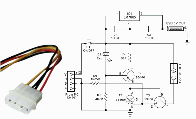
This circuit was designed and manufactured in the 1980s and has functioned without issues since then. It does not present any particular constructional problem, beyond the known: the attention in the provided force of power supply, choice of suitable...
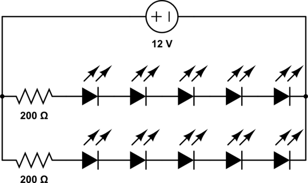
A 12V power supply is available, and there is a need to power LEDs with a forward voltage of 2V. It is questioned whether only six LEDs can be powered or if the cathode of one LED can be...
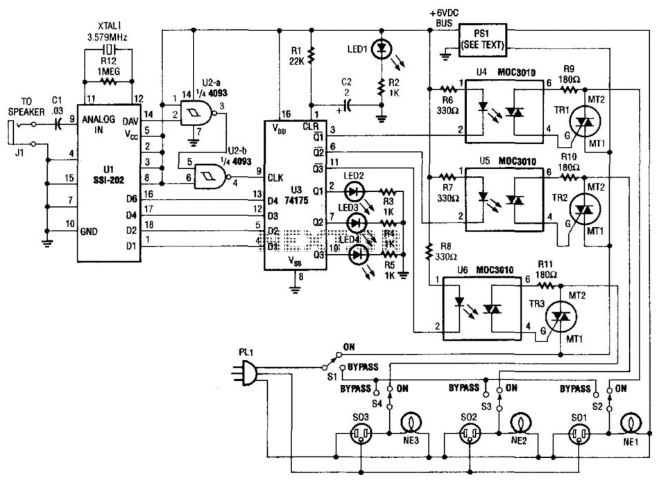
Tones from the DTMF on the telephone line are detected by U1. When a valid tone is received, pin 14 (D More: AV) of U1 produces a positive pulse that is used to drive NAND gates U2A and U2B,...
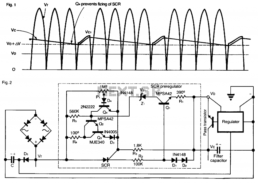
This SCR pre-regulator maintains the filter capacitor voltage (Vc) in a variable output power supply at a few volts above the output voltage (V0). The advantages include reduced heat dissipation by the pass transistor, resulting in a smaller heatsink,...
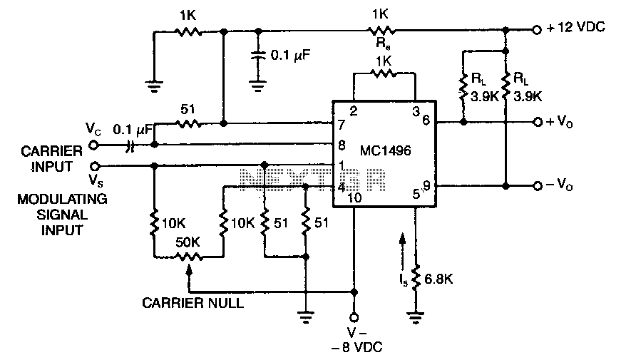
The basic current allows no carrier to be present in the output. By adding offsets to the carrier differential pairs, controlled amounts of carrier appear at the output. The amplitude becomes a function of the modulation signal - AM...