Square·-to-sine-wave-converter

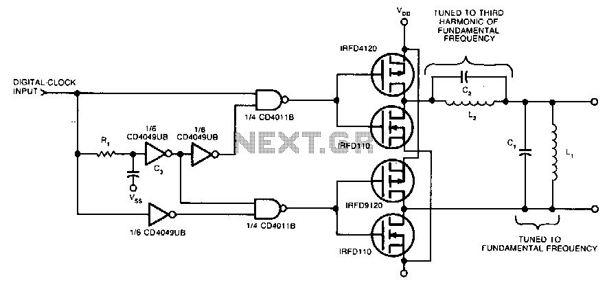
Two pairs of MOSFETs create a bridge that alternately switches current in opposite directions. Two parallel-resonant LC circuits complete the converter. The L1/C1 combination is resonant at the fundamental frequency, while the L2/C2 combination resonates at the third harmonic of the clock frequency and functions as a trap. The transformer T1 and capacitor C3 ensure that both halves of the MOSFET bridge are not activated simultaneously by providing a common delay to the gate drive of each half. More: Select the values of R1 and C3 to achieve a time constant that is less than 5% of the clock's period. An output amplifier can be added for further buffering and conditioning of the circuit's sine-wave output.
The circuit described utilizes a half-bridge configuration of MOSFETs to control the direction of current flow through the load. The use of two pairs of MOSFETs allows for efficient switching, reducing power losses and improving overall performance. The resonant LC circuits play a crucial role in determining the operational characteristics of the converter. The first LC circuit, consisting of inductor L1 and capacitor C1, is tuned to resonate at the fundamental frequency of operation, which facilitates efficient energy transfer. Conversely, the second LC circuit, formed by inductor L2 and capacitor C2, is tuned to resonate at the third harmonic of the clock frequency. This configuration helps to filter out unwanted harmonics and provides a trap for frequencies that could interfere with the desired output waveform.
The transformer T1, in conjunction with capacitor C3, serves a dual purpose. It not only provides isolation between the control circuitry and the power stage but also ensures that the two halves of the MOSFET bridge do not conduct simultaneously. This is critical for preventing shoot-through conditions, which can lead to catastrophic failures in the circuit. The timing of the MOSFET gate drives is controlled such that the delay introduced by the values of resistors R1 and capacitor C3 is less than 5% of the clock period. This ensures that the switching transitions are smooth and that the MOSFETs operate within their safe limits.
To enhance the performance of the circuit, an output amplifier can be integrated. This amplifier will buffer the sine-wave output generated by the LC circuits, providing necessary conditioning to ensure that the output signal meets the required specifications for further processing or load driving. The addition of the output amplifier can also help in driving capacitive loads or in interfacing with subsequent stages of the circuit, thereby improving the overall efficiency and reliability of the system. Proper selection of components and tuning of the circuit parameters are essential for optimizing performance and achieving the desired operational characteristics.Two pairs of MOSFETs form a bridge that alternately switches current in opposite directions. Two parallel-resonant LC circuits complete the converter. The Ll/C1 combination is resonant at the fundamental frequency; the L2/C2 combination is resonant at the clock frequency"s third harmonic and acts as a trap. Tl and C3 ensure that both halves of the MOSFET bridge are never on at the same time by providing a common delay to the gate drive of each half.
Select the values of R1 and C3 to yield a time constant that"s less than 5% of the clock"s period. You can add an output amplifier for additional buffering and conditioning of the circuit"s sine-wave output.