
Tilt Sensor via Accelerometer Circuit

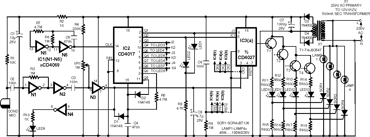
The analog-to-digital conversion circuit is a critical component of the overall project, facilitating the translation of analog signals from sensors into digital data for further processing. The use of LM339 comparators is advantageous due to their reliability and ease of integration into various applications. Each LM339 IC contains four comparators, allowing for efficient utilization of space and resources. In this design, three LM339 ICs are connected in parallel to achieve the required 12 comparator outputs.
The voltage dividers play an essential role in establishing reference voltages for the comparators. The first voltage divider, composed of two equal-value 1kΩ resistors, effectively halves the input voltage from +5V to +2.5V. This reference voltage is crucial for determining the threshold at which the comparators will switch their outputs from logic '0' to logic '1'. The divided voltage is also used to power the accelerometer, ensuring that the entire system operates within the correct voltage range.
The design can potentially be simplified by using fewer components or alternative configurations, which may reduce complexity and improve efficiency. However, the current design prioritizes reliability and ease of troubleshooting, which may justify the additional complexity. Overall, this schematic provides a robust framework for analog-to-digital conversion, enabling accurate data acquisition from the sensors involved in the project.The schematic for this project is fairly large and you can see the complete schematic below. To explain what is happening here I will split it into two sections which I will call the analog and digital sections. The schemtic below (click to enlarge it) is the analog to digital conversion circuit. It has 12 comparators, 6 for the X axis and 6 for the Y axis. These comparators will output a logic `1` when in an active state (previously described in the theory section) otherwise they output a logic `0`. This output is then passed onto the digital circuit where it is parsed. The comparator used for this part of the circuit is the tried and true LM339. It has 4 comparators inside of it and runs off of a single power supply. Since we need 12 comparators in total, 3 LM339 IC`s will be used. Two voltage dividers are used. The first voltage divider is made up of two 1k © resistors which divides the intial +5v down and is then fed to the reference resistor voltage divider.
The divided input voltage turns out to be +2. 25v and it is also used to power the accelerometer. This part of the design could be simplified but I got a little lazy, sorry! 🔗 External reference
Related Circuits
An infra-red or wireless remote control has the disadvantage that the small, handy, remote transmitter is often misplaced. The sound operated switch has the advantage that the transmitter is always with you. This project offers a way to control...
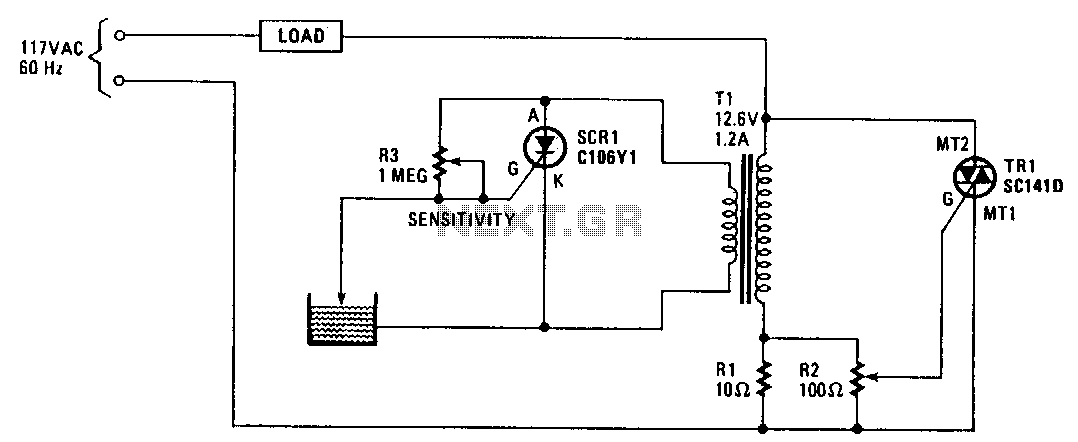
When the water level is low, the probe is out of the water, causing SCR1 to be triggered. This results in the SCR conducting and imposing a significant load on the secondary winding of transformer T1. This load is...
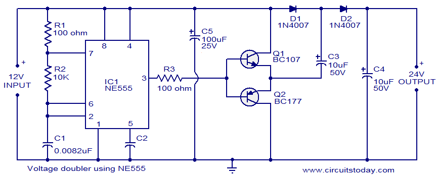
The circuit diagram of a simple voltage doubler using the NE555 timer is presented. In this configuration, the NE555 IC operates as an astable multivibrator at approximately 9 kHz. The bases of two transistors, Q1 and Q2, are connected...
The internal telephone circuit is depicted below. By making minor enhancements to a toy telephone, it can be transformed into a functional internal telephone. This device comprises several components, including the phone unit, a decoding circuit, a ringing circuit,...
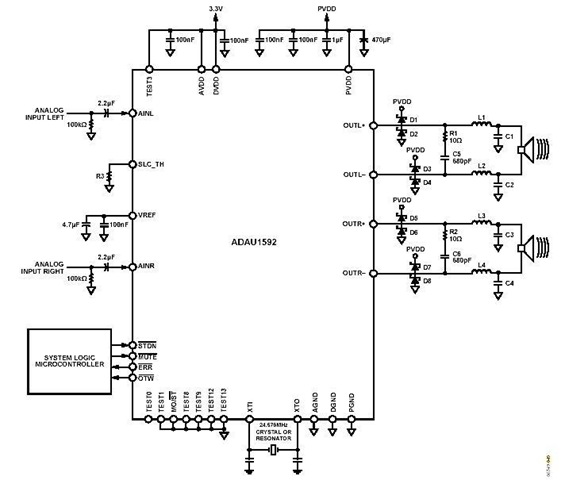
This is a stereo circuit schematic of the ADAU1592, a 2-channel, bridge-tied load (BTL) switching audio power amplifier. The ADAU1592 can be utilized in compact television sets, PC audio systems, and mini-component applications. According to the ADAU1592 datasheet, an...
The objective is to enhance information transmission through the use of articles. Please contact us via email at [email protected] within 15 days if there are any issues related to article content, copyright, or other concerns. Prompt action will be...