
Transformerless Dc -To- Symmetric DC Converter

To achieve dual-polarity supplies, a DC to DC converter will typically utilize a topology that can efficiently generate both positive and negative voltage rails from the single +5V input. One common approach is to use a charge pump or a buck-boost converter.
In a charge pump configuration, capacitors are switched in and out of the circuit to create the necessary voltage levels. This method is advantageous due to its simplicity and compact size. It can provide the required negative voltage by inverting the input voltage, allowing for the generation of both +5V and -5V outputs.
Alternatively, a buck-boost converter can also be employed, which can step down or step up the input voltage. This type of converter typically involves an inductor, a switch (usually a MOSFET), and diodes to control the flow of energy. The buck-boost topology can efficiently provide the desired dual-polarity supplies while maintaining regulation under varying load conditions.
When designing the circuit, it is crucial to consider the load requirements of the op-amps and DACs to ensure that the converter can supply adequate current and maintain voltage stability. Additionally, filtering capacitors should be included on the output to minimize voltage ripple and noise, which is particularly important for analog devices.
Protection features such as overcurrent protection, thermal shutdown, and input/output voltage clamping may also be integrated into the design to enhance reliability and performance. Proper PCB layout techniques should be employed to minimize electromagnetic interference (EMI) and ensure stable operation of the DC to DC converter.A DC to DC converter is needed for a board that only has +5V supply but have to provide dual-polarity supplies for few device such as op-amp or some DAC. Using.. 🔗 External reference
Related Circuits

This power converter is utilized in the LHC machine to supply power to superconductive magnets. It is situated in the underground installation of the LHC, in proximity to the loads to minimize cable losses. The voltage source employs a...
The AD654 is a monolithic voltage-to-frequency (V/F) converter that comprises an input amplifier, a precision oscillator system, and a high-current output stage. A single resistor-capacitor (RC) network is all that is needed to configure any full-scale (FS) frequency up...
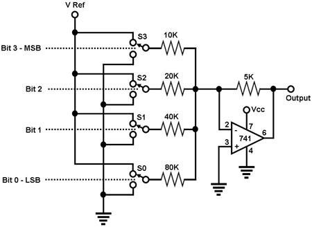
The circuit depicted in Figure 1 is a straightforward 4-bit digital-to-analog converter (DAC). It functions as a simple operational amplifier (op-amp) summer circuit, configured to produce an output voltage that is proportional to the sum of the input voltages....
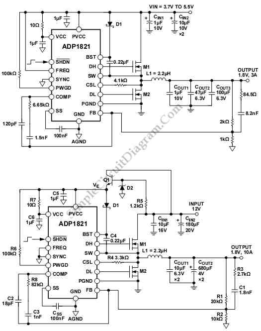
The schematic diagram below illustrates an ADP1821 Step Down DC-to-DC Converter circuit. This circuit employs the ADP1821, which is capable of regulating an output with a load exceeding 20 A, contingent upon the careful selection of power components such...

When the power supply is connected to IC1, the output pin 3 operates at a frequency of 1 kHz. The components Q1 and Q2 work in a push-pull configuration. When a positive output signal is generated, Q1 and Q2...

The operation of the converter is based on the weighted addition and transfer of the analog input levels to the digital output levels. It consists of... The converter functions by utilizing a weighted summation technique to process analog signals and...