
Voltage Doubler and InverterCircuit with Schematic

The MAX660 integrated circuit (IC) is designed for applications requiring a voltage multiplier, specifically functioning as both a voltage doubler and inverter. The circuit utilizes the MAX660 to convert a low input voltage into a higher output voltage, effectively doubling the input voltage while also allowing for inversion of the polarity.
In the voltage doubler configuration, the MAX660 operates by charging capacitors during alternating cycles, which leads to the accumulation of charge and results in a doubled output voltage. The circuit typically includes input and output capacitors, which smooth the voltage output and minimize ripple. The input voltage is applied to the circuit, and through a series of switching actions managed by the IC, the output voltage is generated.
For the voltage inverter operation, the MAX660 is configured to produce a negative output voltage. This is achieved by utilizing the same principles of charge accumulation and capacitor switching, but with the output stage designed to invert the voltage polarity. The inverter circuit is particularly useful in applications requiring a negative supply voltage, such as operational amplifiers or other analog components that necessitate dual supply voltages.
The schematic for both configurations will include the MAX660, input and output capacitors, and potentially additional components such as resistors or diodes to ensure proper operation and stability. The output characteristics can be influenced by the choice of capacitors and the load connected to the output, which should be considered during circuit design to achieve desired performance specifications.
Overall, the MAX660 provides a compact and efficient solution for generating higher voltages and negative voltages from a low-voltage DC source, making it suitable for various electronic applications.Voltage Doubler circuit and Voltage Inverter circuit diagram with schematics using MAX660 IC -which is a DC voltage multiplier IC. This is a dc voltage doubler circuit and inverter.. 🔗 External reference
Related Circuits
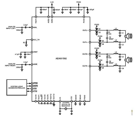
This is a stereo circuit schematic of the ADAU1592, a 2-channel, bridge-tied load (BTL) switching audio power amplifier. The ADAU1592 can be utilized in compact television sets, PC audio systems, and mini-component applications. According to the ADAU1592 datasheet, an...
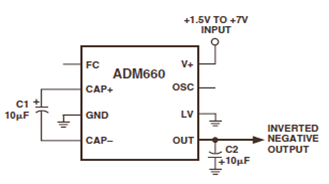
The ADM660 is a charge-pump voltage converter that can either invert the input supply voltage or double it. The schematic below depicts the ADM660 Voltage Inverter Circuit Configuration Diagram. This inverting schematic is ideal for generating a negative rail...
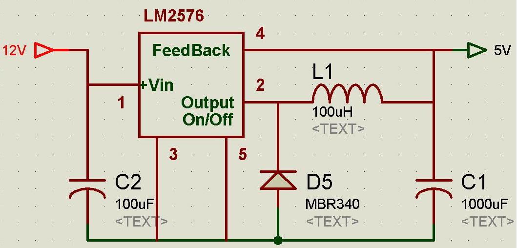
A regulated and noise-free power supply voltage is essential for microcontrollers and other components such as amplifiers, filters, and GPS devices. Voltage surges in the supply voltage can permanently damage embedded systems. A voltage regulator must maintain the output...
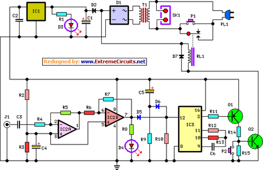
This circuit deactivates an amplifier or any connected device when a low-level audio signal is absent at its input for at least 15 minutes. Activating switch P1 powers the device, enabling operation of any appliance connected to SK1. The...
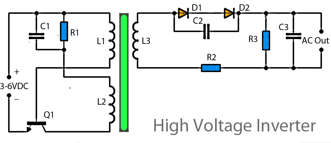
This inverter circuit operates using a transistor and transformer, along with other components, to elevate the voltage. The input supply voltage ranges from 3V to 6V DC, which is then converted to a high voltage AC output. However, the...
This circuit charges two NiCad cells with a constant current and features dual charging rates, voltage cutoff, and an audible alarm. The circuit is powered. This circuit is designed to efficiently charge two nickel-cadmium (NiCad) cells, utilizing a constant current...