
A typical circuit for the LM4910 two-channel amplifier
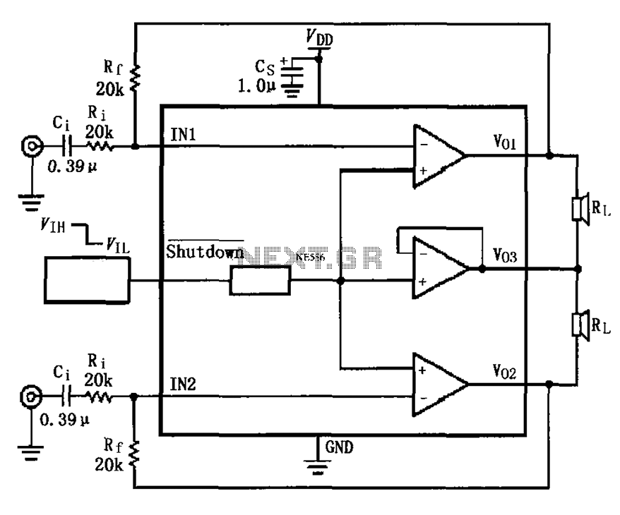
The LM4910 is a dual-channel audio power amplifier optimized for driving small speakers in portable applications. Its compact size and efficient design make it ideal for battery-powered devices. The left and right audio signals are input through pins 1 and 2, where they are processed by the internal circuitry of the amplifier. The gain of the amplifier is set by external resistors, allowing for flexibility in audio output levels.
The output stage of the LM4910 is capable of delivering significant power to the connected speakers, with the maximum power consumption being a crucial consideration in battery-operated designs. The formula PDMAX = 4VDD^2 / (2RL) indicates that the power output is influenced by the supply voltage (VDD) and the load resistance (RL). This relationship is essential for ensuring that the amplifier operates efficiently without exceeding the power capabilities of the connected speakers.
The -3dB bandwidth is an important parameter that defines the frequency response of the amplifier. By selecting appropriate values for the external resistor and capacitor, designers can tailor the performance of the LM4910 to meet specific audio requirements. The input capacitor value of approximately 0.39 µF, derived from the formula, ensures that the amplifier can handle a wide range of audio frequencies while maintaining sound quality.
Additionally, the LM4910 features a control pin (pin 3) that allows for power management in the circuit. This feature is particularly beneficial in portable applications, as it enables the amplifier to be turned off when not in use, conserving battery life. The ability to control the amplifier's operation through a simple high or low signal enhances the versatility of the LM4910 in various electronic designs. Overall, the LM4910 provides a robust solution for audio amplification in compact electronic devices, combining efficiency with high-quality sound output. As shown for the LM4910 typical circuit for two-channel amplifier. Left and right channel audio signals are input LM4910 (MSOP/SO package) 1,2 feet, after an internal amplifier output pin, respectively, by the 8,7,6, added directly to the respective speakers. Amplifier gain Av -Rf/Ri, the maximum power consumption by the PDMAX 4VDD2/2RL. Input of external resistor and capacitor, respectively determine the input -3dB bandwidth taken Ci 1/(2 20k 20Hz), using about 0.39 F capacitor. LM4910 3 feet off the external control, when 3 feet to VDD (high level) when allowed to work, work prohibited ground (low level).
Related Circuits
The alarm protection can trigger a sound and light alert when the mains voltage exceeds or falls below a predetermined threshold. It automatically disconnects the electrical power supply without damaging the electrical protection. The device is compact, fully featured,...
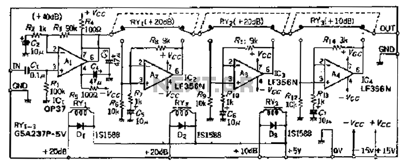
Although the basic amplifier circuit phase AC amplifier remains unchanged, the selection of the correct gain requires the use of series resistors. The circuit does not include a 9kΩ resistor. The input amplifier Ai selected is the OP37, which...
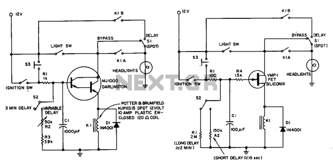
This circuit maintains the headlights of an automobile in an on state temporarily. It also ensures that the lights turn off automatically, even if the user forgets to switch them off manually. The shut-off delay is activated only when...

This circuit is a robust and efficient power amplifier suitable for various audio applications. It delivers 60W RMS output at a 50V supply with an 8 Ohm load. The design is user-friendly, allowing for the use of non-critical components...
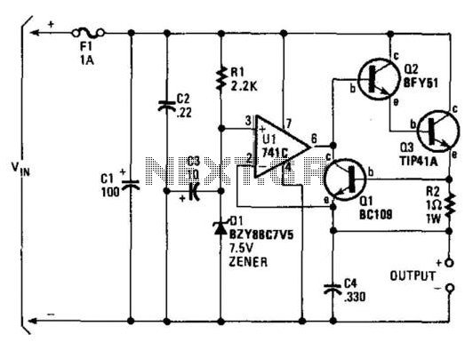
A regulator enables the powering of a 7.5-V cassette recorder or other devices from a 12-V DC automotive system. The circuit can provide approximately 600 mA of current. Q3 requires a heatsink due to its potential to dissipate up...
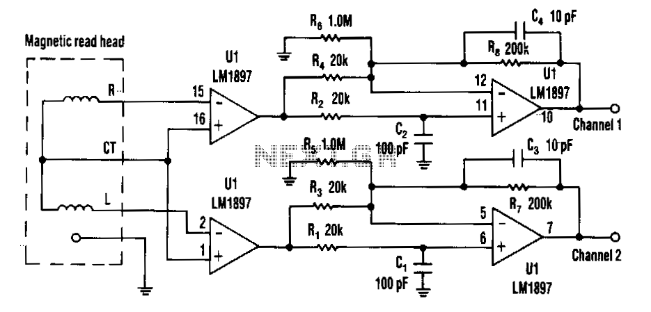
Choosing direct current (DC) coupling instead of alternating current (AC) coupling can significantly reduce the noise associated with preamplifiers for a magnetic reading head, particularly at low frequencies. The LM1897 eliminates the need for the capacitor that typically AC...